Certified Global Research Member


Key Questions Answered
- Global Market Outlook
- In-depth analysis of global and regional trends
- Analyze and identify the major players in the market, their market share, key developments, etc.
- To understand the capability of the major players based on products offered, financials, and strategies.
- Identify disrupting products, companies, and trends.
- To identify opportunities in the market.
- Analyze the key challenges in the market.
- Analyze the regional penetration of players, products, and services in the market.
- Comparison of major players’ financial performance.
- Evaluate strategies adopted by major players.
- Recommendations
Why Choose Market Research Future?
- Vigorous research methodologies for specific market.
- Knowledge partners across the globe
- Large network of partner consultants.
- Ever-increasing/ Escalating data base with quarterly monitoring of various markets
- Trusted by fortune 500 companies/startups/ universities/organizations
- Large database of 5000+ markets reports.
- Effective and prompt pre- and post-sales support.
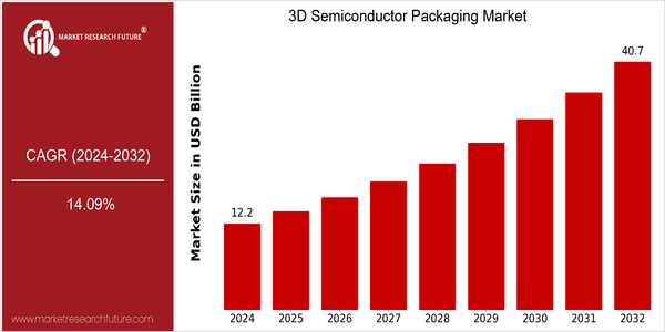
Market Size Snapshot
| Year | Value |
|---|---|
| 2024 | USD 12.2 Billion |
| 2032 | USD 40.7 Billion |
| CAGR (2024-2032) | 14.09 % |
Note – Market size depicts the revenue generated over the financial year
The 3D Semiconductor Packaging Market is poised for significant growth, with a current market size of USD 12.2 billion in 2024, projected to expand to USD 40.7 billion by 2032. This remarkable growth trajectory reflects a compound annual growth rate (CAGR) of 14.09% over the forecast period. The increasing demand for advanced packaging solutions, driven by the proliferation of high-performance computing, artificial intelligence, and the Internet of Things (IoT), is a key factor propelling this market forward. As semiconductor manufacturers seek to enhance performance while minimizing space and power consumption, 3D packaging technologies are becoming increasingly vital. Technological advancements, such as the development of Through-Silicon Vias (TSVs) and advanced interconnects, are further stimulating market growth. Major players in the industry, including Intel, TSMC, and ASE Group, are actively investing in R&D and forming strategic partnerships to innovate and expand their product offerings. For instance, TSMC's recent collaborations with leading tech firms aim to enhance 3D packaging capabilities, ensuring they remain at the forefront of this rapidly evolving market. As these trends continue to unfold, the 3D Semiconductor Packaging Market is set to play a crucial role in shaping the future of electronics and computing.
Regional Market Size
Regional Deep Dive
The 3D Semiconductor Packaging Market is experiencing significant growth across various regions, driven by the increasing demand for miniaturization and enhanced performance in electronic devices. In North America, the market is characterized by a strong presence of leading semiconductor companies and advanced research institutions, fostering innovation and technological advancements. Europe is witnessing a surge in investments in semiconductor manufacturing, particularly in countries like Germany and France, which are focusing on sustainable and efficient packaging solutions. The Asia-Pacific region, particularly China, Japan, and South Korea, is the largest market due to its robust electronics manufacturing base and rapid adoption of advanced packaging technologies. The Middle East and Africa are gradually emerging as potential markets, with increasing investments in technology infrastructure. Latin America, while still developing, shows promise with growing interest in semiconductor applications across various sectors.
Europe
- The European Union has launched the European Chips Act to strengthen the semiconductor supply chain, which includes significant funding for research in advanced packaging technologies, thereby enhancing the region's competitiveness.
- Leading companies like STMicroelectronics and Infineon Technologies are focusing on developing eco-friendly packaging solutions, aligning with the EU's sustainability goals and influencing market dynamics.
Asia Pacific
- China's semiconductor industry is rapidly advancing, with companies like Huawei and TSMC investing in 3D packaging technologies to meet the growing demand for high-performance chips in consumer electronics.
- Japan is focusing on innovation in 3D packaging through collaborations between companies like Sony and various research institutions, aiming to enhance the performance of their semiconductor products.
Latin America
- Brazil is emerging as a key player in the semiconductor market, with government initiatives aimed at boosting local manufacturing capabilities, which may include advancements in 3D packaging technologies.
- Mexico is becoming a manufacturing hub for electronics, with companies like Flex and Jabil expanding their operations, which could drive demand for advanced packaging solutions.
North America
- The U.S. government has initiated the CHIPS Act, which aims to boost domestic semiconductor manufacturing and R&D, directly impacting the 3D semiconductor packaging market by increasing funding and support for innovative packaging technologies.
- Companies like Intel and AMD are investing heavily in 3D packaging technologies, such as Intel's Foveros technology, which allows for stacking chips vertically, enhancing performance and efficiency.
Middle East And Africa
- Countries like Israel are becoming hubs for semiconductor innovation, with companies such as Tower Semiconductor leading the way in advanced packaging technologies, which is expected to attract more investments in the region.
- The UAE is investing in technology parks and initiatives to foster semiconductor development, which could lead to increased adoption of 3D packaging solutions in the region.
Did You Know?
“Did you know that 3D semiconductor packaging can reduce the footprint of electronic devices by up to 50%, allowing for more compact and efficient designs?” — International Journal of Electronics
Segmental Market Size
The 3D Semiconductor Packaging segment plays a crucial role in enhancing the performance and efficiency of electronic devices, and it is currently experiencing significant growth. Key drivers of demand include the increasing need for miniaturization in consumer electronics and the rising complexity of integrated circuits, which necessitate advanced packaging solutions. Additionally, the push for higher performance in computing and telecommunications is propelling the adoption of 3D packaging technologies. Currently, the adoption stage of 3D Semiconductor Packaging is in the scaled deployment phase, with companies like Intel and TSMC leading the charge in implementing these technologies in their products. Notable applications include high-performance computing, mobile devices, and automotive electronics, where 3D packaging enhances functionality and reduces form factor. Trends such as the global shift towards electric vehicles and the growing emphasis on sustainability are further catalyzing the demand for innovative packaging solutions. Technologies like Through-Silicon Vias (TSVs) and advanced die stacking methods are shaping the evolution of this segment, enabling more efficient designs and improved thermal management.
Future Outlook
The 3D Semiconductor Packaging Market is poised for significant growth from 2024 to 2032, with the market value projected to escalate from $12.2 billion to $40.7 billion, reflecting a robust compound annual growth rate (CAGR) of 14.09%. This growth trajectory is primarily driven by the increasing demand for advanced packaging solutions in high-performance computing, artificial intelligence, and the Internet of Things (IoT). As industries continue to push for miniaturization and enhanced performance, 3D packaging technologies, such as Through-Silicon Via (TSV) and System-in-Package (SiP), are expected to gain substantial traction, leading to higher penetration rates in consumer electronics and automotive applications. Key technological advancements, including the integration of heterogeneous integration and advanced materials, will further propel the market. The ongoing shift towards 5G technology and the rising adoption of electric vehicles are anticipated to create new opportunities for 3D semiconductor packaging solutions. Additionally, supportive government policies aimed at fostering semiconductor innovation and manufacturing capabilities will play a crucial role in shaping the market landscape. As a result, by 2032, it is expected that 3D semiconductor packaging will account for a significant share of the overall semiconductor market, driven by its ability to meet the evolving demands of next-generation electronic devices.
Covered Aspects:| Report Attribute/Metric | Details |
|---|---|
| Market Size Value In 2023 | USD 12.2 Billion |
| Growth Rate | 14.09% (2024-2032) |
3D Semiconductor Packaging Market Highlights:
Leading companies partner with us for data-driven Insights
Kindly complete the form below to receive a free sample of this Report
Tailored for You
- Dedicated Research on any specifics segment or region.
- Focused Research on specific players in the market.
- Custom Report based only on your requirements.
- Flexibility to add or subtract any chapter in the study.
- Historic data from 2014 and forecasts outlook till 2040.
- Flexibility of providing data/insights in formats (PDF, PPT, Excel).
- Provide cross segmentation in applicable scenario/markets.