Certified Global Research Member


Key Questions Answered
- Global Market Outlook
- In-depth analysis of global and regional trends
- Analyze and identify the major players in the market, their market share, key developments, etc.
- To understand the capability of the major players based on products offered, financials, and strategies.
- Identify disrupting products, companies, and trends.
- To identify opportunities in the market.
- Analyze the key challenges in the market.
- Analyze the regional penetration of players, products, and services in the market.
- Comparison of major players’ financial performance.
- Evaluate strategies adopted by major players.
- Recommendations
Why Choose Market Research Future?
- Vigorous research methodologies for specific market.
- Knowledge partners across the globe
- Large network of partner consultants.
- Ever-increasing/ Escalating data base with quarterly monitoring of various markets
- Trusted by fortune 500 companies/startups/ universities/organizations
- Large database of 5000+ markets reports.
- Effective and prompt pre- and post-sales support.
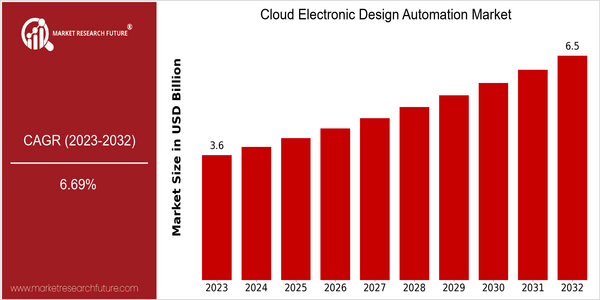
Market Size Snapshot
| Year | Value |
|---|---|
| 2023 | USD 3.63 Billion |
| 2032 | USD 6.5 Billion |
| CAGR (2024-2032) | 6.69 % |
Note – Market size depicts the revenue generated over the financial year
Cloud-based EDA is projected to reach $ 3.1 billion by 2023 and $ 6.5 billion by 2032. This translates into a compound annual growth rate (CAGR) of 6.69% between 2024 and 2032, which shows a strong demand for cloud-based EDA. The complexity of the system and the need for an efficient design process are the main driving forces of this market. The trend of using cloud-based EDA tools is becoming more and more popular as companies seek to improve productivity and reduce time-to-market. Also, the integration of artificial intelligence and machine learning into EDA tools is driving the market. The use of these two new tools helps designers automate complex tasks, optimize their designs and increase their accuracy, thus simplifying the design process. The main players in the market, such as Cadence, Synopsis and Mentor, are investing heavily in research and development, forming strategic alliances and launching new products to take advantage of these new opportunities. Recent alliances between EDA companies and cloud service companies are expected to increase the scalability and accessibility of EDA tools, thereby attracting a larger number of users. The market is expected to grow as the demand for advanced electronic devices increases.
Regional Market Size
Regional Deep Dive
The cloud-based EDA market is growing rapidly in many regions of the world, driven by the growing demand for advanced semiconductors and the growing trend towards cloud-based solutions. North America has a strong presence of leading technology companies and a thriving innovation-driven start-up scene. Europe is seeing strong support for digital transformation from governments. The Asia-Pacific region is adopting cloud-based EDA tools rapidly as a result of its growing manufacturing industry. The Middle East and Africa are also adopting cloud-based EDA tools, albeit at a slower pace, influenced by the differences in the level of development of their IT infrastructure. Latin America is beginning to adopt cloud-based EDA tools, driven by the need for cost-effective design tools in a competitive market.
Europe
- The European Union's Digital Compass initiative aims to accelerate digital transformation across member states, which is likely to drive investments in cloud EDA solutions.
- Companies like Siemens and Dassault Systèmes are leading the charge in integrating AI with cloud EDA tools, enhancing design efficiency and reducing time-to-market for new products.
Asia Pacific
- China's push for self-sufficiency in semiconductor production is leading to increased investments in cloud EDA technologies, with local firms like Huawei and Alibaba entering the market.
- The rise of electric vehicles in countries like Japan and South Korea is creating a demand for advanced electronic designs, further propelling the adoption of cloud EDA solutions.
Latin America
- Brazil's growing tech ecosystem is seeing an increase in cloud EDA adoption as companies seek to modernize their design processes.
- Government initiatives aimed at boosting the local semiconductor industry are expected to create opportunities for cloud EDA providers in the region.
North America
- The U.S. government has launched initiatives to bolster semiconductor manufacturing, which is expected to increase the demand for cloud EDA tools among local companies like Cadence Design Systems and Synopsys.
- Recent partnerships between cloud service providers such as Amazon Web Services and EDA companies are enhancing the accessibility of advanced design tools, making it easier for startups to innovate.
Middle East And Africa
- The UAE's Vision 2021 is promoting innovation and technology adoption, which is gradually fostering interest in cloud EDA tools among local tech firms.
- Emerging startups in South Africa are beginning to leverage cloud EDA solutions to compete in the global market, although infrastructure challenges remain a barrier.
Did You Know?
“Did you know that the global semiconductor industry is projected to reach $1 trillion by 2030, significantly driving the demand for cloud EDA tools?” — International Semiconductor Industry Association
Segmental Market Size
The cloud EDA market is currently experiencing a robust growth phase, mainly driven by the increasing complexity of semiconductors and the need for a faster time-to-market. The need for advanced design tools to support the development of IoT and AI applications is driving this market, as is the trend towards remote collaboration in the design process. Companies like Cadence and Synopsys are at the forefront of this trend and have been able to develop cloud-based tools. The use of cloud EDA tools is currently in a phase of expansion, with notable implementations in North America and Asia-Pacific. Intel and TSMC have already started to integrate cloud EDA tools into their design flows. Among the main applications are the design, verification and test of integrated circuits, where the cloud-based platforms facilitate real-time collaboration and resource sharing. Further growth drivers are the trend towards sustainable semiconductor manufacturing and the digital transformation of industries. In the design phase, machine learning and artificial intelligence are transforming design methodology, making it more efficient and more advanced.
Future Outlook
From 2023 to 2032, the cloud EDA market will grow from $ 3,637,000,000 to $ 6,484,200,000, a 6% CAGR. The growth is driven by the increasing demand for advanced chip technology and the increasing complexity of the circuits and systems, which require the development of advanced design tools. The need for efficient and scalable design solutions in the automotive, telecommunications and consumer electronics industries will drive the EDA tools to be widely used in the cloud, which will enhance the team's collaboration and reduce the time to market for new products. The integration of AI and ML into EDA tools is expected to change the design process, enabling faster simulation and design. In addition, the trend of remote work and the dispersion of teams will also drive the demand for cloud EDA tools, which have the advantages of convenience and access. The government's policy of encouraging innovation in the field of semiconductor design and production will also create a favourable environment for the development of the EDA market. By 2032, cloud EDA tools will account for about 40% of the overall EDA market.
Covered Aspects:| Report Attribute/Metric | Details |
|---|---|
| Growth Rate | 5.7% (2022-2030) |
Cloud Electronic Design Automation Market Highlights:
Leading companies partner with us for data-driven Insights
Kindly complete the form below to receive a free sample of this Report
Tailored for You
- Dedicated Research on any specifics segment or region.
- Focused Research on specific players in the market.
- Custom Report based only on your requirements.
- Flexibility to add or subtract any chapter in the study.
- Historic data from 2014 and forecasts outlook till 2040.
- Flexibility of providing data/insights in formats (PDF, PPT, Excel).
- Provide cross segmentation in applicable scenario/markets.