Flip Chip Technology Market (2025 - 2035)

Flip Chip Technology Market Size, Share and Research Report By Wafer Bumping Process (Copper Pillar, Tin-Lead Eutectic Solder, Lead-Free Solder (SAC), Cu-to-Cu Hybrid Bonding, Gold Stud Bump), By Packaging Technology (FC-BGA, FCCSP / CSP, Fan-Out WLP / Panel-Level, 2.5D Interposer (CoWoS-type), 3D Stacked), By Product (Memory (DRAM, NAND, HBM), CMOS Image Sensor, CPU / MPU, GPU / AI Accelerator, Networking / Switch ASIC, PMIC / Analog), By End-Use Industry (Consumer Electronics & Wearables, Data-Center & Cloud, Automotive & Transportation, Industrial & Robotics, Telecommunications, Aerospace & Defense) and By Region (North America, Europe, Asia-Pacific, South America, Middle East & Africa) – Industry Forecast to 2035.
ID: MRFR/SEM/3938-HCR
200 Pages
Ankit Gupta, Shubham Munde
Last Updated: July 15, 2026
Flip Chip Technology Market
Market Size
Forecast Period2025-2035
CAGR (2025-2035)6.82%
2025 Market SizeUSD 37.98 Billion
2026 Market SizeUSD 40.57 Billion
2035 Market SizeUSD 73.46 Billion
Key Players
ASE Technology Holding
Intel Corporation
TSMC
Amkor Technology
Samsung Electronics
JCET Group
Opportunities
  • Co-Packaged Optics for Data Centers
  • Panel-Level Fan-Out Packaging
  • Emerging Market Semiconductor Assembly Hubs

Flip Chip Technology Market Summary

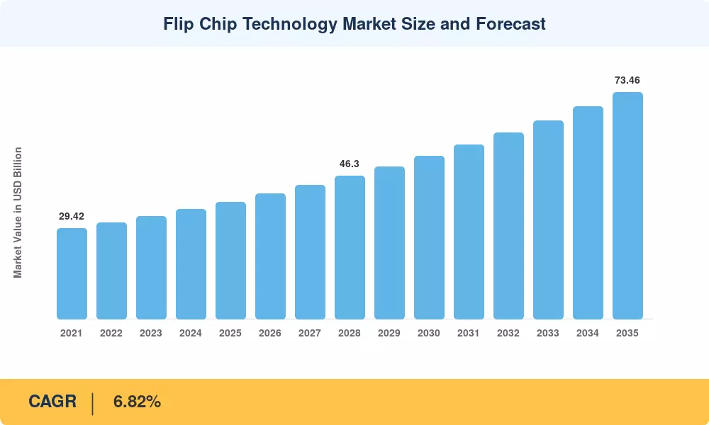
The Flip Chip Technology Market was valued at USD 37.98 billion in 2025 and is projected to reach USD 40.57 billion in 2026, growing to USD 73.46 billion by 2035 at a CAGR of 6.82% during the forecast period (2026–2035). This growth trajectory tracks the semiconductor industry's decisive shift toward chiplet-based system architectures, a transition catalyzed by over USD 52 billion in committed CHIPS Act funding across the United States and the European Chips Act's EUR 43 billion mobilization target [1][2]. Foundry operators and outsourced assembly providers alike are racing to scale packaging capacity, and the Flip Chip Technology Market sits squarely at the center of that race.

The technology landscape within the Flip Chip Technology Market is undergoing a generational transition. Legacy wire-bonding and traditional solder bump processes are giving way to copper-pillar interconnects and, increasingly, Cu-to-Cu hybrid bonding architectures that deliver the sub-10 µm pitch densities demanded by AI accelerators and high-bandwidth memory stacks. Global capital expenditure on advanced packaging lines exceeded USD 8 billion in 2024, a figure expected to double by 2028 as hyperscale cloud operators contract directly with foundries for co-packaged optics and 2.5D/3D integration [3][4].

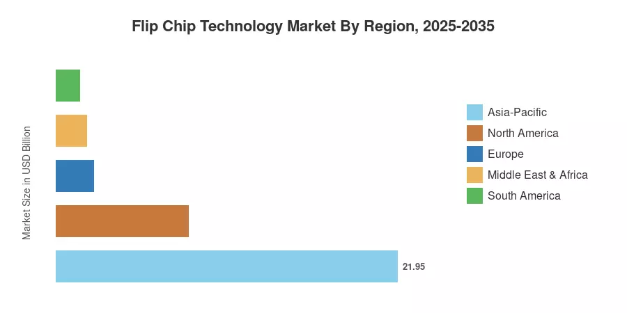
Asia-Pacific commands the dominant position in the Flip Chip Technology Market, capturing approximately 57.8% of 2025 revenue, driven by concentrated OSAT capacity in Taiwan, South Korea, and mainland China. The region is also the fastest-growing, projected to log a CAGR of 8.52% through 2035. North America holds the second-largest share at roughly 22.4%, underpinned by defense-grade packaging demand and the CHIPS Act fab build-outs now materializing in Arizona, Ohio, and Texas. Europe trails at approximately 12.8% share but is accelerating investment through its own semiconductor sovereignty programs.


Key Report Takeaways

• By the Wafer Bumping Process

  • Copper pillar technology held a 49.2% revenue share in the Flip Chip Technology Market in 2025, reflecting its dominance in high-density interconnect applications.
  • Cu-to-Cu hybrid bonding is the fastest-expanding process segment, projected to grow at a 10.3% CAGR through 2035 as sub-5 µm pitch requirements accelerate adoption.

• By Packaging Technology

  • FC-BGA led the Flip Chip Technology Market with a 40.4% share in 2025, driven by server-class processor packaging demand.
  • Fan-out wafer-level and panel-level packaging solutions are forecast to expand at a 10.7% CAGR to 2035.

• By Product

  • Memory devices accounted for 34.2% of the Flip Chip Technology Market share in 2025.
  • GPU and AI accelerator packaging is set to advance at a 13.4% CAGR through 2035, the fastest among product segments.

• By End-Use Industry

  • Consumer electronics and wearables held a 31.1% share of the Flip Chip Technology Market in 2025.
  • Data-center and cloud applications are expected to register an 8.56% CAGR through 2035.

• By Region

  • Asia-Pacific captured 57.8% of the Flip Chip Technology Market in 2025.
  • North America accounted for approximately USD 8.51 billion in 2025 revenue, supported by reshoring initiatives.


Market Size and Forecast (2021–2035)

Market Research Future's sizing methodology triangulates top-down macroeconomic indicators (semiconductor capital expenditure, wafer starts) with bottom-up demand models across packaging process nodes, end-use verticals, and regional capacity utilization data. Historical figures (2021–2024) reflect audited industry data, while the forecast (2026–2035) applies a compound annual growth projection anchored to the 2025 base year.
Flip Chip Technology Market Size and Forecast
Our Impact
Enabled $4.3B Revenue Impact for Fortune 500 and Leading Multinationals
Partnering with 2000+ Global Organizations Each Year
30K+ Citations by Top-Tier Firms in the Industry

Driver Impact Analysis

Driver ~% Impact on CAGR Geographic Relevance Impact Timeline
AI and HPC packaging demand surge +1.8% Global Short-term (≤2 yr)
Chiplet and heterogeneous integration adoption +1.4% North America, Asia-Pacific Medium-term (2–4 yr)
High-bandwidth memory (HBM) generational transitions +1.2% South Korea, Japan Short-term (≤2 yr)
Government semiconductor incentive programs +0.9% North America, Europe Medium-term (2–4 yr)
Automotive electrification and ADAS proliferation +0.7% Europe, China Long-term (≥4 yr)
5G/6G RF front-end module scaling +0.5% Global Medium-term (2–4 yr)
Edge AI and IoT device miniaturization +0.4% Asia-Pacific Long-term (≥4 yr)


AI and HPC Packaging Demand Surge

The single largest catalyst for the Flip Chip Technology Market is the explosive build-out of AI training and inference infrastructure. NVIDIA, AMD, and custom silicon programs at Google, Amazon, and Microsoft collectively consumed an estimated 2.4 million advanced-package units in 2024, a figure that grew over 60% year-on-year [3]. Each next-generation GPU die — whether NVIDIA's Blackwell or AMD's MI400 series — requires larger interposer substrates with higher bump counts, directly expanding addressable flip chip content per device. CoWoS and its equivalents now operate at near-full utilization across TSMC and ASE facilities, creating pricing leverage that sustains margin expansion for the packaging ecosystem [6].

Chiplet and Heterogeneous Integration Adoption

The semiconductor industry's pivot from monolithic die scaling to chiplet-based architectures is fundamentally reshaping the Flip Chip Technology Market. Intel's disaggregated Ponte Vecchio GPU contains over 40 chiplets bonded via EMIB and Foveros technology, while AMD's EPYC processors rely on multi-die flip chip assemblies. The UCIe (Universal Chiplet Interconnect Express) consortium, which reached 1.1 specification status in 2024, is standardizing die-to-die interfaces and lowering integration barriers for fabless firms [8]. This architectural shift increases the number of flip chip bonds per system by 3–5× compared with monolithic alternatives.

High-Bandwidth Memory Generational Transitions

SK hynix, Samsung, and Micron are each investing over USD 10 billion cumulatively in HBM production capacity through 2027, with HBM4 expected to stack 16 DRAM layers using advanced thermal compression bonding [6]. Each HBM stack requires thousands of micro-bump interconnects, making memory packaging one of the highest-volume flip chip applications in the Flip Chip Technology Market. The transition from HBM3E to HBM4 alone is projected to increase bump density by 40%, further tightening supply across advanced packaging lines [8].

Government Semiconductor Incentive Programs

The U.S. CHIPS and Science Act has allocated USD 39 billion in direct manufacturing incentives and USD 13.2 billion in R&D funding, with Intel, TSMC, and Samsung among the primary recipients building advanced packaging capacity on American soil [1]. The European Chips Act targets EUR 43 billion in public and private investment to double the EU's global semiconductor production share to 20% by 2030 [2]. Japan's METI has committed JPY 3.9 trillion (approximately USD 26 billion) to semiconductor supply-chain resilience, including Rapidus Corporation's 2 nm fab and associated packaging lines [11].


Restraints Impact Analysis

The restraint impact estimates below represent directional headwinds to the Flip Chip Technology Market's growth rate. They reflect supply-side constraints, cost structures, and regulatory friction identified through primary research and should not be subtracted directly from the stated CAGR.

Restraint ~% Impact on CAGR Geographic Relevance Impact Timeline
Substrate supply bottlenecks and long lead times –0.6% Global Short-term (≤2 yr)
Thermal management complexity at advanced nodes –0.5% Global Medium-term (2–4 yr)
High capital intensity of hybrid bonding equipment –0.4% North America, Europe Medium-term (2–4 yr)
Export control fragmentation (U.S.–China) –0.4% North America, Asia-Pacific Long-term (≥4 yr)
Skilled workforce shortages in packaging engineering –0.3% Global Long-term (≥4 yr)


Substrate Supply Bottlenecks

ABF (Ajinomoto Build-up Film) substrate availability remains a critical chokepoint for the Flip Chip Technology Market. Lead times for high-layer-count FC-BGA substrates stretched to 50+ weeks during 2023–2024, and while capacity additions by Ibiden, Shinko Electric, and AT&S are coming online, demand from AI accelerator packaging continues to outpace new supply [13]. Substrate costs account for approximately 40–50% of total advanced package cost, and pricing has remained elevated at 15–20% above pre-shortage levels.

Thermal Management Complexity

As die stacks get larger and the density of interconnects increases, thermal dissipation gets exponentially harder. A 16-layer HBM4 stack creates local hotspots above 150 W/cm2, which is a challenge for traditional thermal interface materials [14]. These thermal problems demand co-design of packaging and cooling subsystems with a product development cycle extension of 6–12 months in the Flip Chip Technology Market and a validation cost increase of an estimated 15–20% each program.


Export Control Fragmentation

The semiconductor export limits from the U.S. Bureau of Industry and Security in October 2023, and subsequent modifications in 2024, have limited sales to China of sophisticated packaging equipment and several chiplet technologies [16]. These constraints result in split supply chains, forcing OSATs to maintain distinct process lines and compliance infrastructure. This fragmentation restricts economies of scale and results in regulatory uncertainty that delays investment choices, especially for equipment suppliers with a large revenue exposure in China, for the Flip Chip Technology Market.


Flip Chip Technology Market Opportunities

Co-Packaged Optics for Data Centers

Optical interconnects converging with flip chip packaging is a high-growth adjacency. Co-packaged optics (CPO) embed photonic engines within switch ASICs itself, providing power savings of up to 30% against pluggable transceivers [4]. Broadcom, Marvell and Intel are each developing CPO solutions using flip chip bonding of silicon photonics dies to electrical interposers, which could represent a potential incremental USD 4+ billion opportunity for the Flip Chip Technology Market by 2032.


Panel-Level Fan-Out Packaging

The move from round wafer-based to rectangular panel-based fan-out packaging is predicted to cut the cost per unit area by 40–50% and help surmount the economic hurdle that has constrained fan-out to premium applications [15]. Samsung and Daedeok Electronics have shown panel-level processing of FC-BGA substrates, and industry roadmaps are targeting volume production by 2027-2028. This cost breakthrough will likely propel the Flip Chip Technology Market in mid-tier consumer electronics and automotive applications.


Emerging Market Semiconductor Assembly Hubs

India's Semiconductor Mission, backed by USD 10 billion in government incentives, is attracting OSAT investment from Tata Electronics, CG Power, and international players seeking geographic diversification [11]. Vietnam and Malaysia are similarly expanding their packaging capabilities. These emerging hubs offer labor-cost advantages and supply-chain resilience, presenting a significant growth vector for the Flip Chip Technology Market as companies de-risk concentrated APAC sourcing.

Automotive Chiplet Integration

The average semiconductor content per vehicle is expected to exceed USD 1,200 by 2030, up from roughly USD 700 in 2023 [9]. As automakers adopt zone-based architectures and centralized compute platforms, the demand for automotive-grade flip chip packages — particularly for ADAS SoCs and power management ICs — is expanding rapidly. Qualification cycles remain long (18–24 months), but early movers in the Flip Chip Technology Market stand to capture significant share in this high-reliability segment.

AI-Driven Design and Process Optimization

Machine learning is increasingly applied to flip chip design-rule optimization, bump placement, and defect detection. Synopsys and Siemens EDA have integrated AI-based layout tools that reduce design iterations by 25–30%, compressing time-to-market [10]. This digital transformation creates a new service layer — data-driven process analytics — that OSAT providers can monetize through premium yield-enhancement contracts, adding a recurring-revenue dimension to the Flip Chip Technology Market.


Flip Chip Technology Market Future Outlook

AI-Native Packaging Architectures

The next decade will see the Flip Chip Technology Market shaped by AI workloads that demand packaging solutions engineered from the ground up for massive parallelism and memory bandwidth. The International Energy Agency projects that global data-center electricity consumption will exceed 1,000 TWh by 2030, creating intense pressure to reduce per-operation energy costs through tighter die-to-die integration [18]. Packages that co-locate compute, memory, and optical I/O on a single substrate will command premium pricing and represent the highest-margin opportunity in the market.

Chiplet Ecosystem Standardization

UCIe and other open interconnect standards are expected to create a modular chiplet ecosystem analogous to the PC component market's standardization era. By 2030, an estimated 20–25% of all high-performance logic devices will ship as multi-chiplet assemblies, up from under 5% in 2024 [8]. This standardization lowers entry barriers for fabless designers and broadens the customer base for the Flip Chip Technology Market, particularly as mid-tier foundries adopt interoperable packaging platforms.

Sustainability and Green Packaging

Environmental, social, and governance pressures are reaching semiconductor packaging. Lead-free solder mandates under the EU's updated RoHS Directive, water-use reduction targets at major OSATs, and customer sustainability scorecards from hyperscalers are collectively pushing the Flip Chip Technology Market toward lower-impact processes [19]. Hybrid bonding's elimination of solder materials entirely positions it as the most environmentally favorable interconnect technology at scale.

Regionalized Supply-Chain Architectures

By 2035, the Flip Chip Technology Market will operate within a more geographically distributed supply-chain model. TSMC's plants in Arizona and Kumamoto, Samsung's Taylor, Texas facility, and Intel's Magdeburg fab each include packaging capabilities designed to serve regional customers with reduced lead times [1][2]. The World Semiconductor Trade Statistics organization estimates that non-Asia-Pacific advanced packaging capacity will rise from 12% of the global total in 2024 to over 22% by 2033, reshaping competitive dynamics across the Flip Chip Technology Market [20].


Flip Chip Technology Market Segmentation

By Wafer Bumping Process

Segment Key Metric Primary Demand Driver
Copper Pillar 49.2% share (2025) Fine-pitch logic and GPU packaging
Tin-Lead Eutectic Solder USD 8.42 Billion (2025) Legacy industrial and consumer devices
Lead-Free Solder (SAC) 5.62% CAGR (2026–2035) RoHS compliance in automotive
Cu-to-Cu Hybrid Bonding 10.3% CAGR (2026–2035) Sub-5 µm pitch HPC and memory stacking
Gold Stud Bump USD 1.84 Billion (2025) RF and MEMS sensor packaging


Copper pillar remains the workhorse process in the Flip Chip Technology Market, offering the best balance of current-carrying capacity, electromigration resistance, and manufacturability at pitches between 40 µm and 100 µm. Its dominance spans server processors, networking ASICs, and mobile application processors. Cu-to-Cu hybrid bonding, while still a small share of total revenue, is growing fastest as it enables the direct die stacking required for next-generation HBM and logic-on-logic architectures. TSMC's SoIC platform and Intel's Foveros Direct are the leading vehicles for hybrid bonding commercialization [8].

By Packaging Technology

Segment Key Metric Primary Demand Driver
FC-BGA 40.4% share (2025) Server, HPC, and networking processors
FCCSP / CSP USD 9.18 Billion (2025) Mobile SoCs and connectivity ICs
Fan-Out WLP / Panel-Level 10.7% CAGR (2026–2035) Cost-optimized heterogeneous integration
2.5D Interposer (CoWoS-type) 9.86% CAGR (2026–2035) AI accelerator and HBM integration
3D Stacked 8.94% CAGR (2026–2035) Memory-on-logic and CMOS image sensors


FC-BGA's leadership in the Flip Chip Technology Market reflects its entrenched position in server and PC processor packaging, where Intel and AMD have shipped billions of units over two decades. The format's scalability to large body sizes (up to 100 mm × 100 mm) makes it the default choice for data-center chips. Fan-out WLP and panel-level solutions represent the most disruptive growth vector, targeting cost-sensitive applications where traditional FC-BGA substrates are economically prohibitive [15].

By Product

Segment Key Metric Primary Demand Driver
Memory (DRAM, NAND, HBM) 34.2% share (2025) HBM ramp for AI training clusters
CMOS Image Sensor USD 3.62 Billion (2025) Smartphone multi-camera and automotive vision
CPU / MPU 6.48% CAGR (2026–2035) Server and PC processor refresh cycles
GPU / AI Accelerator 13.4% CAGR (2026–2035) Generative AI infrastructure build-out
Networking / Switch ASIC 7.82% CAGR (2026–2035) 800G/1.6T Ethernet switching
PMIC / Analog USD 2.94 Billion (2025) EV power management and industrial automation


Memory packaging constitutes the largest product category in the Flip Chip Technology Market, driven by the sheer volume of DRAM and NAND flash production and the rapid HBM ramp. GPU and AI accelerator packaging, while smaller in absolute revenue, is the fastest-growing segment, reflecting the industry's capital-intensive race to deploy generative AI infrastructure at scale [3].

By End-Use Industry

Segment Key Metric Primary Demand Driver
Consumer Electronics & Wearables 31.1% share (2025) Smartphone, tablet, and AR/VR device proliferation
Data-Center & Cloud 8.56% CAGR (2026–2035) Hyperscale AI infrastructure expansion
Automotive & Transportation 9.24% CAGR (2026–2035) ADAS, EV power, and infotainment SoCs
Industrial & Robotics USD 4.28 Billion (2025) Factory automation and edge AI controllers
Telecommunications 6.74% CAGR (2026–2035) 5G/6G base station and RF front-end modules
Aerospace & Defense USD 2.16 Billion (2025) Trusted-foundry radar and EW packaging


Consumer electronics drives the largest volume in the Flip Chip Technology Market, though average selling prices per package are lower than in data-center or defense applications. The data-center and cloud segment is rising fastest as hyperscalers invest in custom ASICs and next-generation accelerators that each consume significantly more packaging content than general-purpose processors [3][4].


Regional Market Share Analysis

Region Key Metric Primary Investment Themes
Asia-Pacific 57.8% share (2025) OSAT capacity expansion, HBM production, foundry-led packaging
North America USD 8.51 Billion (2025) CHIPS Act reshoring, defense packaging, AI accelerator demand
Europe 6.38% CAGR (2026–2035) European Chips Act, automotive chiplet integration
South America USD 1.52 Billion (2025) EMS assembly growth, consumer device localization
Middle East & Africa 5.18% CAGR (2026–2035) Sovereign digital programs, defense modernization
Total USD 37.98 Billion (2025)

The Flip Chip Technology Market exhibits significant geographic concentration, with Asia-Pacific anchoring the majority of production capacity and demand. Regional dynamics are shaped by government incentive programs, proximity to major fabless customers, and the density of OSAT infrastructure.


North America

Country Key Metric Key Driver
United States 78.4% of regional share CHIPS Act fab and packaging investments
Canada 5.22% CAGR (2026–2035) Photonics and quantum packaging R&D
Mexico USD 0.42 Billion (2025) Nearshoring EMS expansion


The United States dominates the North American Flip Chip Technology Market, driven by Intel's USD 20 billion Ohio fab complex that includes dedicated advanced packaging halls, TSMC's Arizona facility ramping 4/3 nm wafer production with adjacent CoWoS capacity, and a dense cluster of defense-grade OSAT providers serving Department of Defense trusted-foundry programs [1]. Canada's strength lies in photonic integration research at institutions such as the National Research Council, while Mexico is emerging as a low-cost back-end assembly hub for consumer electronics OEMs.

Europe

Country Key Metric Key Driver
Germany 28.6% of regional share Automotive semiconductor sovereignty
United Kingdom 5.94% CAGR (2026–2035) Compound semiconductor packaging
France USD 0.68 Billion (2025) STMicroelectronics and CEA-Leti R&D
Italy 4.86% CAGR (2026–2035) Power semiconductor packaging
Spain USD 0.21 Billion (2025) Emerging OSAT partnerships
Nordic Countries 5.48% CAGR (2026–2035) RF and sensor packaging
Russia USD 0.14 Billion (2025) Domestic chip production push
Rest of Europe 4.72% CAGR (2026–2035) EU Chips Act spillover


Germany anchors Europe's Flip Chip Technology Market, where Infineon, Bosch, and Continental drive demand for automotive-qualified flip chip packages. The European Chips Act's Pilot Line initiative is funding advanced packaging R&D at IMEC (Belgium) and Fraunhofer IZM (Germany), with a focus on 3D heterogeneous integration for automotive and industrial applications [2].

Asia-Pacific

Country Key Metric Key Driver
China 32.4% of regional share Domestic OSAT expansion and HiSilicon demand
Japan 7.94% CAGR (2026–2035) Rapidus and legacy OSAT modernization
South Korea USD 5.82 Billion (2025) HBM and logic packaging for Samsung and SK hynix
India 9.14% CAGR (2026–2035) Semiconductor Mission greenfield investments
ASEAN USD 2.74 Billion (2025) Malaysia and Vietnam assembly diversification
Rest of Asia-Pacific 6.28% CAGR (2026–2035) Taiwan OSAT dominance (ASE, SPIL)


Asia-Pacific's leadership in the Flip Chip Technology Market reflects the region's unmatched OSAT concentration. Taiwan-based ASE Technology Holding alone processes over 30% of the world's advanced packages, while South Korea's memory giants consume massive volumes of thermal compression bonding capacity for HBM production [6]. China's JCET Group and TongFu Microelectronics are rapidly building domestic capability to offset export-control pressures, with combined capex exceeding USD 3 billion in 2024 [16].

South America

Country Key Metric Key Driver
Brazil 62.5% of regional share Consumer electronics assembly
Argentina USD 0.18 Billion (2025) Government digital infrastructure programs
Rest of South America 4.68% CAGR (2026–2035) Gradual EMS capacity additions


Brazil dominates South America's share of the Flip Chip Technology Market, primarily through EMS operations that assemble consumer devices for the domestic market under Manaus free-trade-zone incentives. Packaging complexity in the region remains lower than in Asia-Pacific, though Brazilian universities are building microelectronics research programs with federal science-ministry funding [11].

Middle East & Africa

Country Key Metric Key Driver
Saudi Arabia 31.8% of regional share Vision 2030 digital economy programs
UAE 6.02% CAGR (2026–2035) Smart-city semiconductor procurement
South Africa USD 0.12 Billion (2025) Mining and industrial IoT packaging demand
Egypt 4.52% CAGR (2026–2035) Electronics manufacturing localization
Rest of MEA USD 0.26 Billion (2025) Defense modernization spending


The Middle East & Africa segment of the Flip Chip Technology Market is nascent but growing, anchored by Saudi Arabia's NEOM and Vision 2030 initiatives that include semiconductor design centers and partnerships with international foundries. The UAE's investment in AI-driven smart-city infrastructure creates downstream demand for packaged processors and sensors, though local assembly capability remains limited [11].


Flip Chip Technology Market By Region, 2025-2035

Competitive Benchmarking

The Flip Chip Technology Market exhibits medium concentration, with an estimated top-five share of 48–55% and a Herfindahl-Hirschman Index in the 900–1,200 range. The landscape features vertically integrated device manufacturers (IDMs), pure-play foundries expanding into packaging, and dedicated OSAT providers. Competition is intensifying as foundries like TSMC and Samsung bring advanced packaging in-house, compressing the addressable market for traditional OSATs.

Company Est. Revenue Share Range Key Offerings for Flip Chip Technology Market Strategic Positioning
ASE Technology Holding ~12–16% FC-BGA, 2.5D/3D, copper pillar bumping Largest global OSAT; full-spectrum packaging
Intel Corporation ~8–12% Foveros, EMIB, hybrid bonding IDM with captive and merchant packaging
TSMC ~7–11% CoWoS, InFO, SoIC Foundry-led advanced packaging leader
Amkor Technology ~7–10% FC-BGA, FCCSP, fan-out WLP Second-largest OSAT; automotive-qualified
Samsung Electronics ~6–9% I-Cube, X-Cube, HBM assembly IDM and foundry with HBM vertical integration
JCET Group ~5–8% FC-CSP, bumping, 2.5D integration Leading Chinese OSAT; domestic supply-chain focus
Powertech Technology ~4–6% Memory packaging, bumping services Memory-centric OSAT aligned with Micron
TongFu Microelectronics ~3–5% FC-BGA, system-in-package Chinese OSAT scaling advanced packaging
Chipbond Technology ~2–4% Bumping, gold stud, testing services Taiwan-based niche bumping specialist
Texas Instruments ~2–4% Flip chip for analog and embedded IDM with captive analog packaging


Recent News & Developments

  • TSMC (March 2025): Announced a USD 100 billion U.S. investment plan including advanced packaging facilities in Arizona, expanding CoWoS capacity to meet AI accelerator demand [1].


  • Samsung Electronics (September 2024): Qualified its 12-layer HBM3E stack using advanced thermal compression bonding, securing supply agreements with major AI chip designers [6].
  • Amkor Technology (July 2024): Broke ground on its first U.S. advanced packaging facility in Peoria, Arizona, supported by USD 2 billion in CHIPS Act preliminary awards [1].


  • U.S. Department of Commerce (October 2023): Finalized updated semiconductor export controls expanding restrictions on advanced packaging equipment and technology transfers to certain countries [16].


Flip Chip Technology Market Report Scope

Parameter Detail
Market Scope Global Flip Chip Technology Market across wafer bumping, packaging technology, product, end-use, and geography
Study Period 2021–2035
CAGR (2026–2035) 6.82%
Base Year Market Size USD 37.98 Billion (2025)
2026 Forecast Start USD 40.57 Billion
2035 Forecast Endpoint USD 73.46 Billion
Fastest Growing Segments GPU/AI Accelerator (by product); Cu-to-Cu Hybrid Bonding (by process); Fan-Out WLP (by technology)
Companies Profiled ASE Technology Holding, Intel, TSMC, Amkor, Samsung, JCET Group, Powertech Technology, TongFu Microelectronics, Chipbond Technology, Texas Instruments
Valuation Currency USD Billion


FAQs

How does hybrid bonding differ from copper-pillar bumping in terms of yield risk?
Hybrid bonding requires sub-100 nm surface planarity and particle-free clean rooms, making defect sensitivity roughly 5–10× higher than copper-pillar processes. Most fabs report hybrid bonding yields between 95% and 98% at mature nodes, narrowing the gap as tool sets improve [15].
Which substrate material trends should procurement teams monitor through 2030?
Glass core substrates are the leading candidate to supplement organic ABF, offering superior dimensional stability and enabling finer redistribution layers. Intel and several substrate vendors are targeting volume glass-core production by 2027 [14].
What is the typical qualification timeline for automotive-grade flip chip packages?
Automotive qualification follows AEC-Q100/104 standards and typically requires 18–24 months of reliability testing, including thermal cycling, HAST, and board-level drop testing. Accelerated programs can compress this to 12 months with early supplier engagement [9].
How are foundries' packaging ambitions affecting OSAT pricing power?
TSMC's and Samsung's in-house packaging expansion is compressing OSAT margins on high-end 2.5D/3D work by 200–400 basis points. OSATs are responding by diversifying into automotive and industrial segments where foundry participation is minimal [20].
What cybersecurity considerations apply to flip chip supply chains?
Hardware Trojans inserted during bumping or underfill steps are a growing concern for defense programs. Trusted-foundry accreditation (DMEA) and die-level traceability using unique physical identifiers are the primary countermeasures [16].
How does panel-level fan-out compare with traditional FC-BGA on total cost of ownership?
Panel-level processing can reduce per-unit packaging cost by 40–50% due to larger substrate utilization and higher throughput. However, warpage control and yield management at panel scale remain engineering challenges [15].
What role does advanced packaging play in reducing AI inference energy consumption?
Tighter die-to-die interconnects cut data-movement energy by 5–10× compared with board-level links. Co-locating memory and logic through 3D stacking can reduce total system power for inference workloads by 25–35% [18].    
Author
Author
Author Profile
Ankit Gupta LinkedIn
Team Lead - Research
Ankit Gupta is a seasoned market intelligence and strategic research professional with over six plus years of experience in the ICT and Semiconductor industries. With academic roots in Telecom, Marketing, and Electronics, he blends technical insight with business strategy. Ankit has led 200+ projects, including work for Fortune 500 clients like Microsoft and Rio Tinto, covering market sizing, tech forecasting, and go-to-market strategies. Known for bridging engineering and enterprise decision-making, his insights support growth, innovation, and investment planning across diverse technology markets.
Co-Author
Co-Author Profile
Shubham Munde LinkedIn
Team Lead - Research
Shubham brings over 7 years of expertise in Market Intelligence and Strategic Consulting, with a strong focus on the Automotive, Aerospace, and Defense sectors. Backed by a solid foundation in semiconductors, electronics, and software, he has successfully delivered high-impact syndicated and custom research on a global scale. His core strengths include market sizing, forecasting, competitive intelligence, consumer insights, and supply chain mapping. Widely recognized for developing scalable growth strategies, Shubham empowers clients to navigate complex markets and achieve a lasting competitive edge. Trusted by start-ups and Fortune 500 companies alike, he consistently converts challenges into strategic opportunities that drive sustainable growth.

Research Approach


Secondary Research

The secondary research process involved comprehensive analysis of regulatory databases, industry standards publications, peer-reviewed engineering journals, and authoritative technology organizations. Key sources included the US Department of Commerce (International Trade Administration), European Commission (Digital Strategy & Chips Act), Semiconductor Industry Association (SIA), IEEE Xplore Digital Library, IPC Association (Connecting Electronics Industries), SEMI (Semiconductor Equipment and Materials International), Taiwan Semiconductor Industry Association (TSIA), China Semiconductor Industry Association (CSIA), Japan Electronics and Information Technology Industries Association (JEITA), Korea Semiconductor Industry Association (KSIA), US Bureau of Industry and Security, National Institute of Standards and Technology (NIST), European Semiconductor Equipment Manufacturers (SEMI Europe), United Nations Comtrade Database, World Trade Organization (WTO) Trade Statistics, and national electronics ministry reports from key markets (Ministry of Industry and Information Technology - China, Ministry of Electronics and Information Technology - India). These sources were used to collect manufacturing statistics, regulatory compliance data, technology standards, patent filings, trade volumes, and market landscape analysis for silicon flip-chip, organic flip-chip, metal flip-chip, and hybrid flip-chip technologies across wafer-level packaging, chip-on-board packaging, flip-chip on laminate, and flip-chip on glass segments.


Primary Research

Qualitative and quantitative insights were obtained by interviewing supply-side and demand-side stakeholders during the primary research process. The supply-side sources consisted of CEOs, VPs of Technology Development, leaders of Advanced Packaging Engineering, and commercial directors from semiconductor manufacturers, OSATs (Outsourced Semiconductor Assembly and Test providers), and equipment/material suppliers. The demand-side sources included chief technology officers from consumer electronics OEMs, automotive electronics leaders, telecommunications equipment procurement leads, and medical device engineering directors from tier-1 manufacturing facilities. Primary research has confirmed technology migration roadmaps and packaging transition timelines, validated market segmentation across consumer electronics, automotive, telecommunication, industrial, and healthcare applications, and gathered insights on wafer-level packaging adoption rates, material pricing strategies for conductive adhesives and underfill materials, and supply chain localization dynamics.

Primary Respondent Breakdown:

By Designation: C-level Primaries (28%), Director Level (42%), Others (30%)

By Region: North America (40%), Europe (22%), Asia-Pacific (30%), Rest of World (8%)


Market Size Estimation

Global market valuation was derived through revenue mapping and wafer-level packaging volume analysis. The methodology included:

Identification of 50+ key manufacturers across North America, Europe, Asia-Pacific, and Latin America, spanning IDMs (Integrated Device Manufacturers), OSATs, and specialized packaging houses

Product mapping across silicon flip-chip, organic flip-chip, metal flip-chip, and hybrid flip-chip categories, with granular segmentation by wafer-level packaging (WLP), chip-on-board (COB), flip-chip on laminate (FCoL), and flip-chip on glass (FCoG) technologies

Analysis of reported and modeled annual revenues specific to flip-chip packaging portfolios, including conductive adhesives, solder balls, underfill materials, and protective coatings segments

Coverage of manufacturers representing 75-80% of global flip-chip packaging market share in 2024, including Intel, TSMC, ASE Technology, Amkor, JCET, and key material suppliers such as Henkel, Indium Corporation, and Namics Corporation

Extrapolation using bottom-up (wafer volume × packaging ASP by technology node and application) and top-down (manufacturer revenue validation across OSAT and IDM segments) approaches to derive segment-specific valuations for consumer electronics, automotive, telecommunications, industrial, and medical device end markets

Download Free Sample

Kindly complete the form below to receive a free sample of this Report

Download PDF ×

We do not share your information with anyone. However, we may send you emails based on your report interest from time to time. You may contact us at any time to opt-out.