Rising Demand for High-Speed Data Transmission
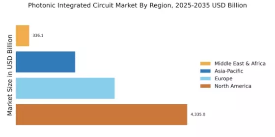
The Global Photonic Integrated Circuit Market Industry is experiencing a surge in demand for high-speed data transmission, driven by the increasing reliance on data centers and cloud computing. As organizations seek to enhance their data processingcapabilities, photonic integrated circuits offer a viable solution due to their ability to transmit data at significantly higher speeds compared to traditional electronic circuits. This trend is reflected in the projected market value of 8.67 USD Billion in 2024, with expectations to reach 49.2 USD Billion by 2035. The compound annual growth rate of 17.1% from 2025 to 2035 underscores the critical role of photonic technology in meeting the evolving needs of global communication networks.
FUTURE DEVELOPMENT DIRECTION OF PIC TECHNOLOGY
Photonic integrated circuits have made significant advances in recent years, both technologically and commercially. In terms of integration, performance, and cost, photonic integrated circuits and electronic integrated circuits still differ greatly. It is anticipated that the following areas will be the primary focus of PIC's future development:
5.5.1 THE USE OF INDIUM PHOSPHIDE MATERIALS
Indium phosphide has limitations as a substrate. Since it is a rare material, InP PIC products are relatively expensive. Furthermore, integrating current silicon-based materials on a large scale is not feasible with indium phosphide as the base material, which will not support the integration of photonic and electronic devices on a large scale in the future. Companies are working hard to make indium phosphide the only material capable of producing large-scale photonic integrated circuits on a commercial scale. Given the current situation, it is unlikely that silicon-based photonics will see significant advancement in the upcoming years. Consequently, it makes sense to develop PICs on a large-scale using indium phosphide material as the substrate. However, there are a lot of technical issues with using indium phosphide. Further research is still needed to determine how to lower costs, simplify the process even more, and enhance integration and chip performance. Common Approaches for Hybrid Integration of InP PICs: (a) Edge-coupling method through active alignment between the PICs (b) Edge-coupling approach employing flip-chip alignment (c) Surface-coupling approach with grating couplers (d) Surface-coupling approach using 45° vertical m Copyright © 2023 Market Research Future 53 FORECAST TO 2030
5.5.2 CONTINUED RESEARCH ON SILICON-BASED LARGE-SCALE PIC
Silicon-based materials are widely used in the fabrication of electronic integrated circuits. Integrated circuits made of silicon have not only been extremely successful commercially, but they have also significantly altered human lifestyles. People have been putting a lot of effort into developing photonic integrated circuits using the advanced technology and methods of electronic integrated circuits since the beginning of PIC technology. Nevertheless, the device is unable to detect light with wavelengths of 1310 nm and 1550 nm due to the extremely low luminous efficiency of silicon-based materials. Furthermore, electro-optic modulation is not possible with it. These significantly impede the advancement of PIC technology based on silicon. The implementation of silicon-based active optical devices through hybrid integration and the investigation of CMOS technology's potential for creating photonic integrated circuits are the primary areas of focus for silicon-based photonic integrated circuit research. Research in this field is being conducted by organizations and research centers like Bell Labs and Intel, and some progress has been made.
5.5.3 FURTHER STUDY ON INTEGRATED OPTICAL LOGIC DEVICES
This is the essential technology needed to make the photonic integrated circuit a reality. In contrast to the photonic logic devices, which are bulky and limited to use in laboratories, electronic logic devices are extremely basic and simple to implement. Even though integrated optical logic device research is still in its early stages, it is still necessary before optical logic signal processing can be put into practice. The true implementation of photonic integrated circuits will only be possible with significant advancements in the integration of optical logic devices. High-speed transmission increases line transmission capacity, and photonic integrated circuits improve device integration. By integrating photonic integrated circuits and high-speed interface, the OTN (Optical Transport Network) device can fully combine the benefits of networking scheduling and bandwidth, resulting in high-quality high-speed link grooming. In the meantime, the implementation of OTN will enable unified end-to-end physical transmission and management and significantly increase network transparency.