PCB design software offers engineers the flexibility to simulate the current design on a computer, allowing them to identify and address issues in real-time. The software provides access to advanced features like auto-placement, auto-routing, and auto-tuning, streamlining the PCB fabrication process and accelerating production. This technology addresses traditional challenges in the PCB industry, such as input signals, desired output, and error tolerance, contributing significantly to industry growth. The increasing demand for PCBs from end-users is exerting substantial pressure on PCB manufacturers. To efficiently design PCBs, manage costs, deliver feature-rich products, achieve product differentiation, and expedite time-to-market, companies are intensifying their investments in the PCB design process. This strategic focus on PCB design is a key driver propelling the growth of the PCB design software market. An illustrative example is the system design tool feature in PCB design software, which facilitates defining and partitioning electronic systems from a logical abstract level to the PCB. Over 33% of best-in-class companies extensively use this software enabler, surpassing the industry average. Virtual prototyping is another heavily utilized feature among PCB manufacturers, minimizing re-spins and enabling the design of higher quality products at faster rates. This tool has become a standard part of product design for many companies, making PCB design software essential for numerous PCB providers. Furthermore, additional features such as design for manufacturability, design collaboration, and design data management are enhancing the necessity of this software, driving market growth globally. The capability to optimize designs for manufacturing, collaborate seamlessly on design projects, and efficiently manage design data has become crucial for the PCB industry. In conclusion, the adoption of PCB design software is instrumental in addressing industry challenges and driving efficiency in the PCB fabrication process. The market is propelled by the increasing demand for PCBs, leading companies to invest significantly in PCB design to meet various requirements such as cost-effectiveness, product differentiation, and swift time-to-market. The extensive use of features like system design tools and virtual prototyping highlights the integral role of PCB design software in the contemporary landscape of electronic product development.
Report Attribute/Metric | Details |
---|---|
Market Opportunities | Increasing Demand for Adoption Of New Technologies |
Market Dynamics | Rise In Need to Reduce Time And Eliminate The Issues Faced During Product Development Extensive Application of PCBS In Various Industries |
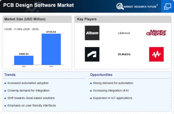
The PCB Design Software Market size is projected to grow from USD 1966.92 Million in 2024 to USD 4816.12 Million by 2032, exhibiting a compound annual growth rate (CAGR) of 11.84% during the forecast period (2024 - 2032). Additionally, the market size for PCB Design Software was valued at USD 1757.75 Million in 2023.
The rise in the need to reduce time and eliminate the issues faced during product development and the extensive application of PCBs in various industries are driving the growth of the market.
FIGURE 1: PCB DESIGN SOFTWARE MARKET VALUE (2019-2032) USD Million
Source: Secondary Research, Primary Research, MRFR Database, and Analyst Review
Covid-19 Analysis
Post-COVID-19, the PCB Design Software market size was valued at USD 1,600.43 Million in 2022 and is projected to reach USD 4,816.12 Million by 2032, growing at a CAGR of 11.9 % from 2023 to 2032. Globally, the pandemic has caused a recession in the economy, forcing companies to drastically restructure their operations. Despite the COVID-19-induced recession affecting industries worldwide, the technology sector suffered less from the crisis than the rest of the economy. The COVID-19 epidemic has had a significant influence on the Global PCB Design Software and people's lives all across the world. Many organizations had waged the struggle on both fronts with zeal. With the advent of a worldwide economic downturn in the millions and trillions of dollars, there was widespread expectation that the major recovery period will extend well into a few more yeyearsThe slow growth rate and a variety of other reasons are to blame for the epidemic. The global pandemic poses various problems to the PCB Design Software Market industry; it affects people worldwide. Significant strategic changes are taking place. MNCs are boosting their investments in response to rising consumer demand worldwide.
With the growing adoption of cutting-edge technologies such as cloud, big data, 3D printing, AI and IoT, various opportunities are researched by PCB software providers to improve the solutions they are providing. Advent of advanced technologies can present lucrative growth opportunities. Portable devices such as smartphones and tablets with features such as increased storage capacity enhanced performance, and better processing speed presents major business opportunities. Furthermore, with advancements in technology, the size of PCB boards is decreasing. Major companies in the market can capitalize on these opportunities and gain a competitive advantage in the market.
Improving PCB design software to cater to varying demands major business opportunities. The complexity and demand for PCB design software are expected to increase, owing to rising demand for smaller devices. For example, one of the opportunities relates to incorporation of various features into a single, consistent interface. This would include making a single program that unites major design, analysis, and documentation features inside a single environment.
Cadence company at present provides many separate products that enable users to run powerful simulations of their PCBs, which are much more powerful than competitor’s tools. But in terms of market demand for integrated PCB design software Altium is leading the market with its offering of single interface integrated with major solutions, which can be seen from Altium’s considerably higher growth compared to Cadence.
Incorporating multiple tools into a single platform improve users’ productivity and increase the range of accessible functionality without investing in multiple programs. For instance, even if the simulation, circuit modelling, and analysis tools integrated into Altium Designer, Altium’s flagship PCB design software package lag behind the tools provide by Cadence and Mentor, still Altium offer more value of money by catering to the demand of integrated software.
On the basis of components, the PCB Design Software market has been divided into Software/Tools and Services. The Software/Tools segment accounted for the largest market share in 2022 and is projected to remain the same during the projected time period. Software or tools are main component of this market which are used by professionals, educators, hobbyists, and others to make a graphic representation and PCB layout by component placement, routing, packaging design and verification to describe the electrical circuits manufactured on a board.
These solutions are used by several industries comprising IT & electronics, mobile devices, healthcare & life science, automotive, telecommunication, transport & logistics, aerospace and defense, research & education, industrial controls automation, and others. The software/tool segment is classified into PCB CAM, PCB SPICE, Cable/Wire Harness, PCB Analysis Tools and PCB AI.
January 2022 Altium launched Nexar, a cloud-based partner platform connecting Altium 365 users with software partners, board fabricators, service providers, component distributors, and manufacturers. Launch of Altimade is the next evolutionary step from the same vision, allowing designers to connect with prototyping and manufacturing partners directly from their design environment.
FIGURE 2: PCB DESIGN SOFTWARE MARKET SHARE BY COMPONENT 2022 VS 2030 (USD Million)
Source: Secondary Research, Primary Research, MRFR Database and Analyst Review
Based on design complexities the PCB Design Software market, has been bifurcated into Low-End Design, Medium-End Design, and High-End Design. The high-end design has largest market share. The commercial or professional PCB packages are mostly utilized by professionals for high-end design. These packages have a high-quality design environment and are involved with high end PCB making consumer and military electronics. The commercial packages are containing various features, for instance, single length tuning, pair routing capability, high speed routing and others. Such packages are featured with built-in simulation solutions along with hierarchical schematic entry. Some of the best high-end design software vendors are Altium Limited, OrCAD, Mentor WG, Pulsonix, The national instruments, Cadence and other.
On the basis of type, the PCB Design Software market has been segmented into PCB Layout and Schematic Capture. PCB layout has largest market share. The PCB layout is a stage after the design of schematic diagram of a PCB. It comprises setting up the design tool, board outline, import of netlist, component placement, routing, silkscreen cleanup, DRC check, and generation of documents for production. PCB layout software greatly help the designers to make highly efficient PCBs due to number of benefits such as reduction of complications of design, early fixation of errors, saving of time & money and ease of use. The growing demand of PCBs in various sectors is forcing PCB manufacturers to take help from this layout software for faster production rate, which is the major factor for the high growth of this segment.
On the basis of deployment, the PCB Design Software market has been bifurcated into cloud and on-premise. On premise has the largest market share. On-premises or desktop software must be installed on local machine of a company. These types of software function without the need of internet connection. Some of the most widespread on-premise PCB design platforms are Altium Designer, CircuitMaker, Eagle, KiCad, and OrCAD. This software is heavy-duty software packages with a ton of features and require a license to run a full-featured version. Most of these are Windows, Mac, and Linux compatible and usually any PCB work will require regular data storage, sharing, retrieval, and occasional software updates in the computer system itself.
The PCB Design Software Market, on the basis of Industry, has been divided into Transportation, Consumer Electronics, Telecommunication, semiconductors, Aerospace and Defence, Healthcare, Industrial Automation & Control, and Education and Research. Telecommunication has the largest market share. Increasing demand for PCB design software in the telecommunication industry and increasing need to save time and production cost are key factors driving growth of the PCB Design Software Market.
By using PCB design software in the telecommunication industry, engineers can digitally detect potential problems in cell towers, satellites, high-speed routers and servers, and commercial phone technologies. In addition, PCB design software are used in mobile phone tower systems, wireless communication systems, cell and tower transmission electronics, and telephonic switching systems to boost signal strength. PCBs are necessary equipment for the telecommunications industry.
By Region, the study segments the market into North America, Europe, Asia-Pacific, Middle East & Africa, and South America. Throughout the forecast period, the North American PCB Design Software market is expected to be dominant. This region's growth is expected to be spearheaded by economies such as Canada and the United States. North America is the dominating the global semiconductor market in terms of chip design and semiconductor R&D. In chip design, the major success factors in USA are access to highly skilled engineering human source and a strong innovation ecosystem, leading by universities. For instance,10 out of the top 20 semiconductor design companies (comprising both fabless and IDMs (Integrated Device Manufacturers)), along with 4 of the top 5 EDA and core IP enterprises by 2019 revenue, are headquartered in the US.
Asia-Pacific is the fastest growing region. The increase in the scope of R&D expenditures in the semiconductor industry by various countries and growing purchaser surmise and flourish demand of consumer electronics are driving the growth of the EDA market in the Asia Pacific region. The positive PCB manufacturing in the region have significant market share, heavy demand of electronics products in emerging countries and government supports to provide favorable environment for semiconductor industry is driving the growth of PCB design software market in Asia-pacific.
Europe is expected to register a significantly rapid revenue growth rate during the forecast period owing to increasing implementation of PCB design software in the electronics sector. Rising demand of PCB design software in the field of telecommunications is also boosting market growth. Germany is the most important actor in the EDA European market, followed by UK. Even in the case of the European industry, electronic components and systems are strong supporters of the development of innovation and productivity in the entire European market and the PCB manufacturers are mainly involved in producing high end PCBs with sophisticated design, but lack in low and medium end PCBs as market is acquired by Asian countries.
In case of the Middle East and Africa, most of the electronics equipment demand is fulfilled by import of Asia-pacific region due to lack of financial and human resources, political unrest, lack of investment and high cost in developing required infrastructure. Still due to presence of number of emerging countries such as Nigeria, South Africa and Israel, there is steady growth in the demand of PCBs in this region which is expected to imitate and propel the growth of PCB design software market in this region.
FIGURE 3: PCB DESIGN SOFTWARE MARKET VALUE BY REGION 2022 VS 2032 (USD Million)
Source: Secondary Research, Primary Research, MRFR Database, and Analyst Review
Further, the countries considered in the scope of the PCB Design Software market are the US, Canada, Mexico, UK, Germany, France, Italy, Spain, Switzerland, Austria, Belgium, Denmark, Finland, Greece, Hungary, Italy, Luxembourg, Netherlands, Norway, Poland, Portugal, Slovakia, Sweden, Romania, Ireland, China, Japan, Singapore, Malaysia, Indonesia, Philippines, South Korea, Hong Kong, Macau, Singapore, Brunei, India, Australia & New Zealand, South Africa, Egypt, Nigeria, Saudi Arabia, Qatar, United Arab Emirates, Bahrain, Kuwait, and Oman, Brazil, Argentina, Chile, and others.
Major market players are spending a lot of money on R&D to increase their product lines, which will help the PCB Design Software market grow even more. Market participants are also taking a range of strategic initiatives to grow their worldwide footprint, including new product launches, contractual agreements, mergers and acquisitions, increased investments, and collaboration with other organizations. Competitors in the PCB Design Software industry must offer cost-effective items to expand and survive in an increasingly competitive and rising market environment.
Cadence Design Systems, Inc. product categories include Functional Verification, Digital integrated circuits (IC) Design and Signoff, Custom IC Design and Verification, System Interconnect and Analysis, and intellectual property (IP). Functional verification products are used to verify that the circuitry or the software designed to perform as intended. Digital IC design offerings are used to create representations of a digital circuit or an IC that can be verified for correctness prior to implementation. Custom IC design and verification offerings are used to create schematic and physical representations of circuits down to the transistor level for analog and memory designs. System Interconnect and Analysis offerings are used to develop printed circuit boards and IC packages. Design IP offerings consist of functional blocks, which customers integrate into their ICs for the development process.
January 2022 Zuken and SnapEDA, a provider of verified online electronic components, are announcing a new capability that provides eCADstar users direct access to SnapEDA’s online library.
June 2021 Cadence Design Systems, Inc debuted the Cadence Allegro X Design Platform, the industry’s first engineering platform for system design that unifies schematic, layout, analysis, design collaboration and data management. Built upon proven Allegro and OrCAD core technology, the new Allegro X platform revolutionizes and streamlines the system design process for engineers—offering unparalleled collaboration across all engineering disciplines, integration with best-in-class Cadence signoff-level simulation and analysis products, and greater layout performance.
© 2024 Market Research Future ® (Part of WantStats Reasearch And Media Pvt. Ltd.)