• Cat-intel
  • MedIntelliX
  • Resources
  • About Us
  • English
    Chinese
    French
    Japanese
    Korean
    German
    Spanish

    Wafer Level Packaging Market Size

    ID: MRFR/SEM/10774-HCR
    128 Pages
    Snehal Singh
    September 2025

    Wafer Level Packaging Market Research Report Information By Type (3D TSV WLP, 2.5D TSV WLP, WLCSP, Nano WLP and Others), By Technology (Fan in wafer level packaging and Fan out wafer level packaging), By End-User (Consumer Electronics, IT and Telecommunication, Automotive and Healthcare), and By Region (North America, Europe, Asia-Pacific, And Rest Of The World) –Industry Forecast Till 2034

    Share:
    Download PDF ×

    We do not share your information with anyone. However, we may send you emails based on your report interest from time to time. You may contact us at any time to opt-out.

    Wafer Level Packaging Market Infographic
    $ 4,950.0
    $ 5,950.0
    $ 7,250.0

    Wafer Level Packaging Size

    Wafer Level Packaging Market Growth Projections and Opportunities

    WLP's market for wafer back-end production and other related products is constantly under numerous kinds of impetus, with various factors defining the direction of it all; this affects demand, technology development and semiconductor industry growth. Wafer-level packaging is closely linked to the miniaturization trend sweeping across electronics. With electronic devices getting increasingly smaller and more compact, even higher-level packaging technologies such as wafer level packaging are required to keep up with the changing form factors. Connecting a number of functions and components in one semiconductor package is an important force behind wafer-level packaging. Selecting an interlayer spacing based on these considerations is one way to glean the best performance out of a chip. It also allows for shorter lengths in wiring connections and greater speed throughout electronic devices, thereby increasing efficiency overall. Portable and wearable electronic devices, from smartphones to IoT (Internet of Things) are increasingly popular in the market. So wafer-level packaging is also stimulated by greater demand for these applications. Because these applications require compact and lightweight packages, WLP is essential to semiconductor manufacturers. The development and adoption of wafer-level packaging is also influenced by advances in semiconductor manufacturing technologies such as advanced lithography, improved materials. Innovative manufacturing processes also help to make WLP solutions scalable and cost effective. The arrival of 5G boosts the need for high-performance semiconductors with greater processing speeds. Whether in 5G applications or elsewhere, performance requirements are very demanding. Wafer-level packaging can improve signal integrity and reduce parasitic effects. The demand for interconnection between networked devices and the proliferation of Internet of Things (IoT) applications fuel this market. WLP can produce compact, low-energy consuming semiconductor devices for a wide range of IoT applications from smart home products to industrial sensors. However, fan-out wafer-level packaging (FO-WLP) is a great step forward in the market. Increased flexibility in placing semiconductor components, better heat dissipation and electrical characteristics: these are reasons why fo-wlp is increasingly gaining importance for high performance applications. As the automotive industry's use of electronics and semiconductor components continues to increase, demand for wafer-level packaging also grows. WLP solutions are designed to satisfy the demanding needs of automotive applications: dependability, miniaturization and long service life in extreme conditions. As environmental issues and regulations affect the wafer-level packaging market, customers progressively turn to lead-free packaging solutions. In choosing materials and manufacturing processes, manufacturers and end-users are both looking for environmentally friendly packaging solutions. Design and packaging trends in the global semiconductor industry, among other factors such as mergers and acquisitions or technological alliances, form a competitive environment for wafer-level packaging. These include strategic collaborations and industry developments that affect market dynamics.

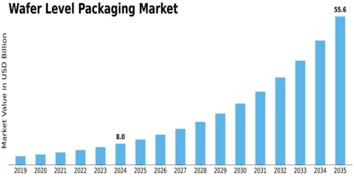
    Wafer Level Packaging Market Size Graph

    Market Summary

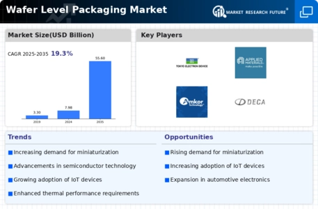
    As per Market Research Future Analysis, the Global Wafer Level Packaging Market was valued at USD 7.98 Billion in 2024 and is projected to reach USD 46.61 Billion by 2034, growing at a CAGR of 19.3% from 2025 to 2034. The market is driven by advancements in the semiconductor industry, increased consumer electronics usage, and demand for ultra-thin wafers. The 2.5D TSV WLP segment leads in market share due to its enhanced capacity and performance. North America dominates the market, followed by Europe and Asia-Pacific, with significant growth expected in the latter region due to rising disposable incomes and smartphone adoption.

    Key Market Trends & Highlights

    Key trends driving the wafer level packaging market include the rise of IoT and panel-level packaging technologies.

    • The wafer level packaging market is expected to grow from USD 9.52 Billion in 2025 to USD 46.61 Billion by 2034.
    • The 2.5D TSV WLP segment is projected to expand rapidly due to its low power consumption and improved performance.
    • North America is the largest market, driven by demand for energy-efficient and compact packaging solutions.
    • Asia-Pacific is anticipated to grow at the fastest CAGR, fueled by increased smartphone adoption and disposable incomes.

    Market Size & Forecast

    2024 Market Size USD 7.98 Billion
    2025 Market Size USD 9.52 Billion
    2034 Market Size USD 46.61 Billion
    CAGR (2025-2034) 19.3%
    Largest Regional Market Share in 2024 North America

    Major Players

    Key players in the wafer level packaging market include Fujitsu, Qualcomm Technologies, Inc., Tokyo Electron Ltd., Jiangsu Changjiang Electronics Technology Co. Ltd, Applied Materials, Inc., Amkor Technology, Inc., Lam Research Corporation, ASML Holding N.V, Toshiba Corporation, and Deca Technologies.

    Market Trends

    Growing usage of semiconductor ICs in the Internet of Things (IoT) is driving the market growth

    The main driver of the expansion of the wafer level packaging market is the increasing use of semiconductor ICs in the Internet of Things (IoT). The adoption of 3G/4G/5G telecommunication standards, government incentives to deploy energy-efficient systems and solutions, and advancements in wired and wireless communication technologies are the main factors driving demand for these IoT devices. IoT chipset demand will increase as more IoT applications are developed and added to IoT devices. These IoT devices use chipsets that incorporate Wi-Fi, RF, FOWLP units (MCU), and sensor modules.

    The demand for thin-profile semiconductor ICs and modules with a reduced footprint is growing rapidly in the semiconductor packaging business as a result of the rapid uptake of mobile and IoT devices. In order to pack IoT chipsets on a smaller footprint, this will increase demand for wafer level packaging technology. IoT device use is increasing, which will fuel market expansion globally over the course of the projection period.

    Another key trend driving the expansion of the worldwide wafer level packaging market is the rise in panel-level packaging. The semiconductor business has undergone several developments as a result of the rising demand for low-cost, high-performance goods. Fan-out panel-level packaging is one of the cutting-edge technologies that has assisted in lowering the overall cost of wafer level packaging. This involves shifting the entire packaging procedure to a large-size panel format, which lowers the overall cost of packaging by enabling the packing of more components on the substrate at once.

    OSAT businesses, IDMs, substrate producers, and fabless businesses all want this technology since it drastically lowers their manufacturing costs. The rising demand for electronics across several industries also makes panel-level packaging a necessity for suppliers to achieve high-volume manufacturing. Thus, driving the wafer level packaging market revenue.

    The ongoing evolution of semiconductor technology suggests that advancements in wafer level packaging are likely to enhance device performance while reducing manufacturing costs, thereby driving broader adoption across various applications.

    U.S. Department of Commerce

    Wafer Level Packaging Market Market Drivers

    Market Growth Projections

    Increased Investment in R&D

    The Global Wafer Level Packaging Market Industry benefits from heightened investment in research and development by key industry players. Companies are increasingly allocating resources to innovate and enhance WLP technologies, aiming to improve yield rates and reduce production costs. This focus on R&D not only fosters technological advancements but also encourages collaboration among stakeholders, including semiconductor manufacturers and packaging service providers. Such investments are crucial for maintaining competitive advantages in a rapidly evolving market landscape. The ongoing commitment to R&D is expected to sustain growth and drive the market towards its projected future value.

    Growth in IoT and Smart Devices

    The proliferation of Internet of Things (IoT) devices significantly contributes to the expansion of the Global Wafer Level Packaging Market Industry. As smart devices become ubiquitous in homes and industries, the need for efficient and compact packaging solutions intensifies. WLP technology offers enhanced performance and thermal management, which are critical for IoT applications. The market's growth is indicative of the increasing integration of WLP in various sectors, including automotive and healthcare, where reliability and efficiency are paramount. This trend is expected to propel the market towards an estimated value of 55.6 USD Billion by 2035.

    Rising Demand for Miniaturization

    The Global Wafer Level Packaging Market Industry experiences a surge in demand driven by the trend towards miniaturization in electronic devices. As consumer electronics evolve, manufacturers seek smaller, lighter, and more efficient components. Wafer Level Packaging (WLP) allows for the integration of multiple functionalities into a single package, thereby reducing size without compromising performance. This trend is particularly evident in smartphones and wearable technology, where space is at a premium. The market is projected to reach 7.98 USD Billion in 2024, reflecting the industry's response to these evolving consumer preferences.

    Advancements in Semiconductor Technology

    Technological advancements in semiconductor manufacturing processes are pivotal to the growth of the Global Wafer Level Packaging Market Industry. Innovations such as 3D packaging and heterogeneous integration enable the development of more complex and efficient semiconductor devices. These advancements facilitate higher performance levels and lower power consumption, which are essential for modern applications. As manufacturers adopt these cutting-edge technologies, the demand for WLP solutions is likely to increase, further driving market growth. The anticipated CAGR of 19.3% from 2025 to 2035 underscores the potential for continued expansion in this sector.

    Regulatory Support for Advanced Packaging Solutions

    Regulatory frameworks supporting advanced packaging solutions play a significant role in shaping the Global Wafer Level Packaging Market Industry. Governments worldwide are recognizing the importance of innovative packaging technologies in enhancing electronic device performance and sustainability. Initiatives aimed at promoting environmentally friendly manufacturing practices encourage the adoption of WLP, which often results in reduced material usage and waste. This regulatory support not only fosters market growth but also aligns with global sustainability goals. As regulations evolve, the demand for advanced packaging solutions is likely to increase, further propelling the market forward.

    Market Segment Insights

    Wafer Level Packaging Type Insights

    The wafer level packaging market segmentation, based on type includes 3D TSV WLP, 2.5D TSV WLP, WLCSP, Nano WLP and Others. The 2.5D TSV WLP segment dominated the market. The 2.5D TSV WLP is used widely because of its enhanced capacity, decreased system space requirements, improved performance, and low power consumption. In the years ahead, this factor would contribute to this segment's market-wide expansion being more rapid.

    Wafer Level Packaging Technology Insights

    The wafer level packaging market segmentation, based on technology, includes Fan in wafer level packaging and Fan out wafer level packaging. The fan in wafer level packaging category generated the most income. Fan-in WLP technology's dominance in the semiconductor industry, which provides indisputable advantages in terms of shape and cost, is credited with the segment's continued expansion. In addition, the variety of fan-in WLP systems keeps growing because to advancements in technology and innovation.

    Source: Secondary Research, Primary Research, MRFR Database and Analyst Review

    Wafer Level Packaging End-User Insights

    The wafer level packaging market segmentation, based on end-user, includes Consumer Electronics, IT and Telecommunication, Automotive and Healthcare. The consumer electronics category generated the most income. The development of electronic packaging technology, which has led to the creation of extremely effective and reliable electrical connecting methods for electronic devices, is responsible for the segment's steady expansion.

    Get more detailed insights about Wafer Level Packaging Market Research Report - Global Forecast 2034

    Regional Insights

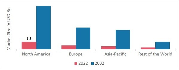
    By region, the study provides the market insights into North America, Europe, Asia-Pacific and Rest of the World. The North American wafer level packaging market area will dominate this market. Due to the demand for energy-efficient, high-performing, and small-form factor packages, WLP is increasingly being used in smaller devices such as smartphones. Additionally, the country is home to a number of top producers of electronic packaging, which is helping the market grow.

    Further, the major countries studied in the market report are The US, Canada, German, France, the UK, Italy, Spain, China, Japan, India, Australia, South Korea, and Brazil.

    Figure 2: WAFER LEVEL PACKAGING MARKET SHARE BY REGION 2022 (USD Billion)

    WAFER LEVEL PACKAGING MARKET SHARE BY REGION 2022

    Source: Secondary Research, Primary Research, MRFR Database and Analyst Review

    Europe wafer level packaging market accounts for the second-largest market share. The growth may be a result of significant manufacturers' growing investments in the mass production of complex semiconductor devices. Additionally, enterprises are using WLP technology to produce goods for the automotive and aerospace industries, which will significantly increase market growth. Further, the German wafer level packaging market held the largest market share, and the UK wafer level packaging market was the fastest growing market in the European region

    The Asia-Pacific Wafer Level Packaging Market is expected to grow at the fastest CAGR from 2024 to 2032. Due to increased disposable incomes in the market, the Asia Pacific area will continue to experience an increase in wafer level packaging demand. The market for wafer-level packaging would be able to face a turbulent increase in demand thanks to India's expanding smartphone adoption. More emphasis will be placed in this area on the production of wafer level packaging.

    Moreover, China’s wafer level packaging market held the largest market share, and the Indian wafer level packaging market was the fastest growing market in the Asia-Pacific region.

    Key Players and Competitive Insights

    Leading market players are investing heavily in research and development in order to expand their product lines, which will help the wafer level packaging market, grow even more. Market participants are also undertaking a variety of strategic activities to expand their footprint, with important market developments including new product launches, contractual agreements, mergers and acquisitions, higher investments, and collaboration with other organizations. To expand and survive in a more competitive and rising market climate, wafer level packaging industry must offer cost-effective items.

    Manufacturing locally to minimize operational costs is one of the key business tactics used by manufacturers in the wafer level packaging industry to benefit clients and increase the market sector. In recent years, the wafer level packaging industry has offered some of the most significant advantages to medicine. Major players in the wafer level packaging market are attempting to increase market demand by investing in research and development operations includes Fujitsu, Qualcomm Technologies, Inc., Tokyo Electron Ltd., Jiangsu Changjiang Electronics Technology Co. Ltd, Applied Materials, Inc., Amkor Technology, Inc., Lam Research Corporation, ASML Holding N.V, Toshiba Corporation, and Deca Technologies.

    Amkor Technology Inc. (Amkor) offers solutions and services for semiconductor packaging and testing. The business provides complete system-level and final test services, as well as turnkey packaging and test services for semiconductor wafers, including bumping, back-grinding, packing, wafer probing, package design, and drop-shipping. It benefits contract foundries, original equipment manufacturers, integrated device makers (IDMs), and fabless semiconductor firms. The artificial intelligence, automotive, communications, computer, consumer, industrial, internet of things, and networking industries all find use for Amkor's products.

    Offering equipment for semiconductor fabrication, ASML Holding NV (ASML) is a provider of microelectronics solutions. equipment for lithography, metrology and inspection, and remanufactured equipment are all part of the company's product line. The company's computational lithography and patterning control software solutions help clients achieve high yield and improved operating efficiency. The foundries, NAND-flash memory, and DRAM memory chip industries are all target markets for ASML's products.

    Key Companies in the Wafer Level Packaging Market market include

    Industry Developments

    March 2023: For the networking and mobile sectors, ASE Inc. recently introduced its newly created advanced fan-out package-on-package (FoPoP) solutions. The company developed this technology to provide low latency and high bandwidth benefits for consumer electronics applications.

    Future Outlook

    Wafer Level Packaging Market Future Outlook

    The Wafer Level Packaging Market is projected to grow at a 19.3% CAGR from 2024 to 2035, driven by advancements in semiconductor technology, increasing demand for miniaturization, and the proliferation of IoT devices.

    New opportunities lie in:

    • Invest in R&D for advanced materials to enhance packaging efficiency and reliability.
    • Develop strategic partnerships with IoT manufacturers to integrate WLP solutions.
    • Expand into emerging markets with tailored WLP products for local industries.

    By 2035, the Wafer Level Packaging Market is expected to achieve substantial growth, solidifying its critical role in the semiconductor industry.

    Market Segmentation

    Wafer Level Packaging Type Outlook

    • 3D TSV WLP
    • 2.5D TSV WLP
    • WLCSP
    • Nano WLP
    • Others

    Wafer Level Packaging End-User Outlook

    • Consumer Electronics
    • IT and Telecommunication
    • Automotive
    • Healthcare

    Wafer Level Packaging Regional Outlook

    • US
    • Canada

    Wafer Level Packaging Technology Outlook

    • Fan In Wafer Level Packaging
    • Fan Out Wafer Level Packaging

    Report Scope

    Report Attribute/Metric Details
    Market Size 2024 USD 7.98 Billion
    Market Size 2025 USD 9.52 Billion
    Market Size 2034 USD 46.61 Billion
    Compound Annual Growth Rate (CAGR) 19.3% (2025-2034)
    Base Year 2024
    Market Forecast Period 2025-2034
    Historical Data 2020- 2023
    Market Forecast Units Value (USD Billion)
    Report Coverage Revenue Forecast, Market Competitive Landscape, Growth Factors, and Trends
    Segments Covered Type, Technology, End-User, and Region
    Geographies Covered North America, Europe, Asia Pacific, and the Rest of the World
    Countries Covered The US, Canada, German, France, UK, Italy, Spain, China, Japan, India, Australia, South Korea, and Brazil
    Key Companies Profiled Fujitsu, Qualcomm Technologies, Inc., Tokyo Electron Ltd., Jiangsu Changjiang Electronics Technology Co. Ltd, Applied Materials, Inc., Amkor Technology, Inc., Lam Research Corporation, ASML Holding N.V, Toshiba Corporation, Deca Technologies
    Key Market Opportunities Ongoing R&D to improve cutting-edge packaging technologies
    Key Market Dynamics Increased use of IoT and AI technologies in the automobile sector Spread of 5G technology in developing countries

    Market Highlights

    Author

    Snehal Singh
    Assistant Manager - Research

    She holds an experience of about 6+ years in market research and business consulting, working under the spectrum of information communication technology, telecommunications and semiconductor domains. aarti conceptualizes and implements a scalable business strategy and provides strategic leadership to the clients. her expertise lies in market estimation, competitive intelligence, pipeline analysis, customer assessment, etc.

    Leave a Comment

    Latest Comments

    John Doe

    This is a great article! Really helped me understand the topic better.

    Posted on July 23, 2025, 10:15 AM
    Jane Smith

    Thanks for sharing this. I’ve bookmarked it for later reference.

    Posted on July 22, 2025, 7:45 PM

    FAQs

    How much is the wafer level packaging market?

    The wafer level packaging market size was valued at USD 7.98 Billion in 2024.

    What is the growth rate of the wafer level packaging market?

    The market is projected to grow at a CAGR of 19.3% during the forecast period, 2025-2034.

    Which region held the largest market share in the wafer level packaging market?

    North America had the largest share in the market

    Who are the key players in the wafer level packaging market?

    The key players in the market are Fujitsu, Qualcomm Technologies, Inc., Tokyo Electron Ltd., Jiangsu Changjiang Electronics Technology Co. Ltd, Applied Materials, Inc., Amkor Technology, Inc., Lam Research Corporation, ASML Holding N.V, Toshiba Corporation, Deca Technologies.

    Which end-user led the wafer level packaging market?

    The consumer electronics category dominated the market in 2022.

    Which type had the largest market share in the wafer level packaging market?

    The 2.5D TSV WLP category had the largest share in the market.

    1. TABLE OF CONTENTS
    2. EXECUTIVE SUMMARY
    3. MARKET INTRODUCTION
      1. Definition
      2. Scope of the Study
        1. Research
    4. Objective
      1. Assumptions
        1. Limitations
    5. RESEARCH METHODOLOGY
      1. Overview
      2. Data Mining
      3. Secondary Research
      4. Primary Research
        1. Primary
    6. Interviews and Information Gathering Process
      1. Breakdown of Primary
    7. Respondents
      1. Forecasting Model
      2. Market Size Estimation
        1. Bottom-Up Approach
        2. Top-Down Approach
    8. Data Triangulation
      1. Validation
    9. MARKET DYNAMICS
      1. Overview
      2. Drivers
      3. Restraints
    10. Opportunities
    11. MARKET FACTOR ANALYSIS
      1. Value Chain Analysis
      2. Porter’s Five Forces Analysis
        1. Bargaining Power
    12. of Suppliers
      1. Bargaining Power of Buyers
        1. Threat
    13. of New Entrants
      1. Threat of Substitutes
        1. Intensity
    14. of Rivalry
      1. COVID-19 Impact Analysis
        1. Market Impact
    15. Analysis
      1. Regional Impact
        1. Opportunity and Threat
    16. GLOBAL WAFER LEVEL PACKAGING MARKET, BY TYPE
    17. Overview
      1. 3D TSV WLP
      2. 2.5D TSV WLP
    18. WLCSP
      1. Nano WLP
      2. Others
    19. GLOBAL WAFER
    20. LEVEL PACKAGING MARKET, BY TECHNOLOGY
      1. Overview
      2. Fan
    21. In Wafer Level Packaging
      1. Fan Out Wafer Level Packaging
    22. GLOBAL WAFER LEVEL PACKAGING MARKET, BY END-USER
      1. Overview
      2. Consumer Electronics
      3. IT and Telecommunication
      4. Automotive
      5. Healthcare
    23. GLOBAL WAFER LEVEL PACKAGING
    24. MARKET, BY REGION
      1. Overview
      2. North America
        1. US
        2. Canada
      3. Europe
        1. Germany
        2. France
        3. UK
        4. Italy
    25. Spain
      1. Rest of Europe
      2. Asia-Pacific
    26. China
      1. India
        1. Japan
        2. South Korea
        3. Australia
        4. Rest of Asia-Pacific
    27. Rest of the World
      1. Middle East
        1. Africa
        2. Latin America
    28. COMPETITIVE LANDSCAPE
      1. Overview
      2. Competitive Analysis
      3. Market Share Analysis
      4. Major Growth Strategy in the Global Wafer Level Packaging Market,
      5. Competitive Benchmarking
      6. Leading Players in Terms of Number
    29. of Developments in the Global Wafer Level Packaging Market,
      1. Key
    30. developments and Growth Strategies
      1. New Technology Launch/Service
    31. Deployment
      1. Merger & Acquisitions
        1. Joint
    32. Ventures
      1. Major Players Financial Matrix
        1. Sales
    33. & Operating Income, 2022
      1. Major Players R&D Expenditure.
    34. 2022
    35. COMPANY PROFILES
      1. Fujitsu
    36. Company Overview
      1. Financial Overview
        1. Products
    37. Offered
      1. Key Developments
        1. SWOT Analysis
        2. Key Strategies
      2. Qualcomm Technologies, Inc.
        1. Company Overview
        2. Financial Overview
    38. Products Offered
      1. Key Developments
        1. SWOT Analysis
        2. Key Strategies
      2. Tokyo Electron Ltd.
        1. Financial Overview
        2. Products
        3. Key Developments
        4. SWOT Analysis
        5. Key Strategies
      3. Jiangsu Changjiang Electronics Technology
    39. Co. Ltd
      1. Company Overview
        1. Financial Overview
        2. Products Offered
        3. Key Developments
    40. SWOT Analysis
      1. Key Strategies
      2. Applied Materials,
    41. Inc
      1. Company Overview
        1. Financial Overview
        2. Products Offered
        3. Key Developments
        4. Key Strategies
      2. Amkor Technology,
        1. Company Overview
        2. Financial Overview
        3. Products Offered
        4. Key Developments
        5. Key Strategies
      3. Lam Research Corporational
        1. Company Overview
        2. Financial Overview
        3. Products Offered
        4. Key Developments
        5. Key Strategies
      4. ASML Holding N.V
        1. Company Overview
        2. Financial Overview
        3. Products Offered
        4. Key Developments
        5. Key Strategies
      5. Toshiba Corporation
        1. Company Overview
        2. Financial Overview
        3. Products Offered
        4. Key Developments
        5. Key Strategies
      6. Deca Technologies
        1. Company Overview
        2. Financial Overview
        3. Products Offered
        4. Key Developments
        5. Key Strategies
    42. APPENDIX
      1. References
      2. Related Reports
    43. LIST OF TABLES
    44. TABLE 1 GLOBAL WAFER LEVEL PACKAGING MARKET, SYNOPSIS, 2025-2034
    45. TABLE 2 GLOBAL WAFER LEVEL PACKAGING MARKET, ESTIMATES & FORECAST, 2025-2034
    46. (USD BILLION)
    47. TABLE 3 GLOBAL WAFER LEVEL PACKAGING MARKET, BY TYPE, 2025-2034
    48. TABLE 4 GLOBAL WAFER LEVEL PACKAGING MARKET, BY TECHNOLOGY,
    49. 2034 (USD BILLION)
    50. TABLE 5 GLOBAL WAFER LEVEL PACKAGING MARKET,
    51. BY END-USER, 2025-2034 (USD BILLION)
    52. TABLE 6 NORTH AMERICA: WAFER LEVEL
    53. PACKAGING MARKET, BY TYPE, 2025-2034 (USD BILLION)
    54. TABLE 7 NORTH AMERICA:
    55. WAFER LEVEL PACKAGING MARKET, BY TECHNOLOGY, 2025-2034 (USD BILLION)
    56. TABLE
    57. NORTH AMERICA: WAFER LEVEL PACKAGING MARKET, BY END-USER, 2025-2034 (USD BILLION)
    58. TABLE 9 US: WAFER LEVEL PACKAGING MARKET, BY TYPE, 2025-2034 (USD BILLION)
    59. TABLE 10 US: WAFER LEVEL PACKAGING MARKET, BY TECHNOLOGY, 2025-2034 (USD
    60. BILLION)
    61. TABLE 11 US: WAFER LEVEL PACKAGING MARKET, BY END-USER, 2025-2034
    62. TABLE 12 CANADA: WAFER LEVEL PACKAGING MARKET, BY TYPE,
    63. TABLE 13 CANADA: WAFER LEVEL PACKAGING MARKET,
    64. BY TECHNOLOGY, 2025-2034 (USD BILLION)
    65. TABLE 14 CANADA: WAFER LEVEL PACKAGING
    66. MARKET, BY END-USER, 2025-2034 (USD BILLION)
    67. TABLE 1 EUROPE: WAFER LEVEL
    68. TABLE 2 EUROPE: WAFER
    69. LEVEL PACKAGING MARKET, BY TECHNOLOGY, 2025-2034 (USD BILLION)
    70. EUROPE: WAFER LEVEL PACKAGING MARKET, BY END-USER, 2025-2034 (USD BILLION)
    71. TABLE 4 GERMANY: WAFER LEVEL PACKAGING MARKET, BY TYPE, 2025-2034 (USD BILLION)
    72. TABLE 5 GERMANY: WAFER LEVEL PACKAGING MARKET, BY TECHNOLOGY, 2025-2034
    73. TABLE 6 GERMANY: WAFER LEVEL PACKAGING MARKET, BY END-USER,
    74. TABLE 7 FRANCE: WAFER LEVEL PACKAGING MARKET,
    75. BY TYPE, 2025-2034 (USD BILLION)
    76. TABLE 8 FRANCE: WAFER LEVEL PACKAGING
    77. MARKET, BY TECHNOLOGY, 2025-2034 (USD BILLION)
    78. TABLE 9 FRANCE: WAFER
    79. LEVEL PACKAGING MARKET, BY END-USER, 2025-2034 (USD BILLION)
    80. TABLE 10
    81. ITALY: WAFER LEVEL PACKAGING MARKET, BY TYPE, 2025-2034 (USD BILLION)
    82. ITALY: WAFER LEVEL PACKAGING MARKET, BY TECHNOLOGY, 2025-2034 (USD BILLION)
    83. TABLE 12 ITALY: WAFER LEVEL PACKAGING MARKET, BY END-USER, 2025-2034 (USD
    84. TABLE 13 SPAIN: WAFER LEVEL PACKAGING MARKET, BY TYPE, 2025-2034
    85. TABLE 14 SPAIN: WAFER LEVEL PACKAGING MARKET, BY TECHNOLOGY,
    86. TABLE 15 SPAIN: WAFER LEVEL PACKAGING MARKET,
    87. TABLE 16 UK: WAFER LEVEL PACKAGING
    88. MARKET, BY TYPE, 2025-2034 (USD BILLION)
    89. TABLE 17 UK: WAFER LEVEL PACKAGING
    90. TABLE 18 UK: WAFER LEVEL
    91. PACKAGING MARKET, BY END-USER, 2025-2034 (USD BILLION)
    92. TABLE 19 REST
    93. OF EUROPE: WAFER LEVEL PACKAGING MARKET, BY TYPE, 2025-2034 (USD BILLION)
    94. TABLE 20 REST OF EUROPE: WAFER LEVEL PACKAGING MARKET, BY TECHNOLOGY, 2025-2034
    95. TABLE 21 REST OF EUROPE: WAFER LEVEL PACKAGING MARKET,
    96. TABLE 22 ASIA-PACIFIC: WAFER LEVEL
    97. TABLE 23 ASIA-PACIFIC:
    98. ASIA-PACIFIC: WAFER LEVEL PACKAGING MARKET, BY END-USER, 2025-2034 (USD BILLION)
    99. TABLE 25 JAPAN: WAFER LEVEL PACKAGING MARKET, BY TYPE, 2025-2034 (USD BILLION)
    100. TABLE 26 JAPAN: WAFER LEVEL PACKAGING MARKET, BY TECHNOLOGY, 2025-2034 (USD
    101. TABLE 27 JAPAN: WAFER LEVEL PACKAGING MARKET, BY END-USER, 2025-2034
    102. TABLE 28 CHINA: WAFER LEVEL PACKAGING MARKET, BY TYPE,
    103. TABLE 29 CHINA: WAFER LEVEL PACKAGING MARKET,
    104. TABLE 30 CHINA: WAFER LEVEL PACKAGING
    105. TABLE 31 INDIA: WAFER LEVEL
    106. TABLE 32 INDIA: WAFER
    107. INDIA: WAFER LEVEL PACKAGING MARKET, BY END-USER, 2025-2034 (USD BILLION)
    108. TABLE 34 AUSTRALIA: WAFER LEVEL PACKAGING MARKET, BY TYPE, 2025-2034 (USD
    109. TABLE 35 AUSTRALIA: WAFER LEVEL PACKAGING MARKET, BY TECHNOLOGY,
    110. TABLE 36 AUSTRALIA: WAFER LEVEL PACKAGING MARKET,
    111. TABLE 37 SOUTH KOREA: WAFER LEVEL
    112. TABLE 38 SOUTH KOREA:
    113. SOUTH KOREA: WAFER LEVEL PACKAGING MARKET, BY END-USER, 2025-2034 (USD BILLION)
    114. TABLE 40 REST OF ASIA-PACIFIC: WAFER LEVEL PACKAGING MARKET, BY TYPE, 2025-2034
    115. TABLE 41 REST OF ASIA-PACIFIC: WAFER LEVEL PACKAGING MARKET,
    116. TABLE 42 REST OF ASIA-PACIFIC:
    117. WAFER LEVEL PACKAGING MARKET, BY END-USER, 2025-2034 (USD BILLION)
    118. REST OF THE WORLD: WAFER LEVEL PACKAGING MARKET, BY TYPE, 2025-2034 (USD BILLION)
    119. TABLE 44 REST OF THE WORLD: WAFER LEVEL PACKAGING MARKET, BY TECHNOLOGY,
    120. TABLE 45 REST OF THE WORLD: WAFER LEVEL PACKAGING
    121. TABLE 46 MIDDLE EAST: WAFER
    122. LEVEL PACKAGING MARKET, BY TYPE, 2025-2034 (USD BILLION)
    123. TABLE 47 MIDDLE
    124. EAST: WAFER LEVEL PACKAGING MARKET, BY TECHNOLOGY, 2025-2034 (USD BILLION)
    125. TABLE 48 MIDDLE EAST: WAFER LEVEL PACKAGING MARKET, BY END-USER, 2025-2034 (USD
    126. TABLE 49 AFRICA: WAFER LEVEL PACKAGING MARKET, BY TYPE, 2025-2034
    127. TABLE 50 AFRICA: WAFER LEVEL PACKAGING MARKET, BY TECHNOLOGY,
    128. TABLE 51 AFRICA: WAFER LEVEL PACKAGING MARKET,
    129. TABLE 52 LATIN AMERICA: WAFER LEVEL
    130. TABLE 53 LATIN AMERICA:
    131. LATIN AMERICA: WAFER LEVEL PACKAGING MARKET, BY END-USER, 2025-2034 (USD BILLION)
    132. LIST OF FIGURES
    133. FIGURE 1 RESEARCH PROCESS
    134. FIGURE 2
    135. MARKET STRUCTURE FOR THE GLOBAL WAFER LEVEL PACKAGING MARKET
    136. FIGURE 3
    137. MARKET DYNAMICS FOR THE GLOBAL WAFER LEVEL PACKAGING MARKET
    138. FIGURE 4
    139. GLOBAL WAFER LEVEL PACKAGING MARKET, SHARE (%), BY TYPE, 2025
    140. FIGURE
    141. GLOBAL WAFER LEVEL PACKAGING MARKET, SHARE (%), BY TECHNOLOGY, 2025
    142. GLOBAL WAFER LEVEL PACKAGING MARKET, SHARE (%), BY END-USER, 2025
    143. GLOBAL WAFER LEVEL PACKAGING MARKET, SHARE (%), BY REGION, 2025
    144. NORTH AMERICA: WAFER LEVEL PACKAGING MARKET, SHARE (%), BY REGION, 2025
    145. FIGURE 9 EUROPE: WAFER LEVEL PACKAGING MARKET, SHARE (%), BY REGION, 2025
    146. FIGURE 10 ASIA-PACIFIC: WAFER LEVEL PACKAGING MARKET, SHARE (%), BY REGION, 2025
    147. FIGURE 11 REST OF THE WORLD: WAFER LEVEL PACKAGING MARKET, SHARE (%), BY
    148. REGION, 2025
    149. FIGURE 12 GLOBAL WAFER LEVEL PACKAGING MARKET: COMPANY SHARE
    150. ANALYSIS, 2025 (%)
    151. FIGURE 13 FUJITSU: FINANCIAL OVERVIEW SNAPSHOT
    152. FIGURE 14 FUJITSU: SWOT ANALYSIS
    153. FIGURE 15 QUALCOMM TECHNOLOGIES,
    154. INC.: FINANCIAL OVERVIEW SNAPSHOT
    155. FIGURE 16 QUALCOMM TECHNOLOGIES, INC.:
    156. FIGURE 17 TOKYO ELECTRON LTD.: FINANCIAL OVERVIEW SNAPSHOT
    157. FIGURE 18 TOKYO ELECTRON LTD.: SWOT ANALYSIS
    158. FIGURE 19 JIANGSU
    159. CHANGJIANG ELECTRONICS TECHNOLOGY CO. LTD: FINANCIAL OVERVIEW SNAPSHOT
    160. FIGURE 20 JIANGSU CHANGJIANG ELECTRONICS TECHNOLOGY CO. LTD: SWOT ANALYSIS
    161. FIGURE 21 APPLIED MATERIALS, INC: FINANCIAL OVERVIEW SNAPSHOT
    162. APPLIED MATERIALS, INC: SWOT ANALYSIS
    163. FIGURE 23 AMKOR TECHNOLOGY,
    164. INC: FINANCIAL OVERVIEW SNAPSHOT
    165. FIGURE 24 AMKOR TECHNOLOGY, INC: SWOT
    166. FIGURE 25 LAM RESEARCH CORPORATIONAL: FINANCIAL OVERVIEW SNAPSHOT
    167. FIGURE 26 LAM RESEARCH CORPORATIONAL: SWOT ANALYSIS
    168. FIGURE 27
    169. ASML HOLDING N.V: FINANCIAL OVERVIEW SNAPSHOT
    170. FIGURE 28 ASML HOLDING
    171. N.V: SWOT ANALYSIS
    172. FIGURE 29 TOSHIBA CORPORATION: FINANCIAL OVERVIEW
    173. SNAPSHOT
    174. FIGURE 30 TOSHIBA CORPORATION: SWOT ANALYSIS
    175. DECA TECHNOLOGIES: FINANCIAL OVERVIEW SNAPSHOT
    176. FIGURE 32 DECA TECHNOLOGIES:

    Wafer Level Packaging Market Segmentation

    Wafer Level Packaging Type Outlook (USD Billion, 2020-2034)

    • 3D TSV WLP
    • 2.5D TSV WLP
    • WLCSP
    • Nano WLP
    • Others

    Wafer Level Packaging Technology Outlook (USD Billion, 2020-2034)

    • Fan In Wafer Level Packaging
    • Fan Out Wafer Level Packaging

    Wafer Level Packaging End-User Outlook (USD Billion, 2020-2034)

    • Consumer Electronics
    • IT and Telecommunication
    • Automotive
    • Healthcare

    Wafer Level Packaging Regional Outlook (USD Billion, 2020-2034)

    • North America Outlook (USD Billion, 2020-2034)
      • North America Wafer Level Packaging by Type
        • 3D TSV WLP
        • 2.5D TSV WLP
        • WLCSP
        • Nano WLP
        • Others
      • North America Wafer Level Packaging by Technology
        • Fan In Wafer Level Packaging
        • Fan Out Wafer Level Packaging
      • North America Wafer Level Packaging by End-User
        • Consumer Electronics
        • IT and Telecommunication
        • Automotive
        • Healthcare
      • US Outlook (USD Billion, 2020-2034)
      • US Wafer Level Packaging by Type
        • 3D TSV WLP
        • 2.5D TSV WLP
        • WLCSP
        • Nano WLP
        • Others
      • US Wafer Level Packaging by Technology
        • Fan In Wafer Level Packaging
        • Fan Out Wafer Level Packaging
      • US Wafer Level Packaging by End-User
        • Consumer Electronics
        • IT and Telecommunication
        • Automotive
        • Healthcare
      • Canada Outlook (USD Billion, 2020-2034)
      • Canada Wafer Level Packaging by Type
        • 3D TSV WLP
        • 2.5D TSV WLP
        • WLCSP
        • Nano WLP
        • Others
      • Canada Wafer Level Packaging by Technology
        • Fan In Wafer Level Packaging
        • Fan Out Wafer Level Packaging
      • Canada Wafer Level Packaging by End-User
        • Consumer Electronics
        • IT and Telecommunication
        • Automotive
        • Healthcare
    • Europe Outlook (USD Billion, 2020-2034)
      • Europe Wafer Level Packaging by Type
        • 3D TSV WLP
        • 2.5D TSV WLP
        • WLCSP
        • Nano WLP
        • Others
      • Europe Wafer Level Packaging by Technology
        • Fan In Wafer Level Packaging
        • Fan Out Wafer Level Packaging
      • Europe Wafer Level Packaging by End-User
        • Consumer Electronics
        • IT and Telecommunication
        • Automotive
        • Healthcare
      • Germany Outlook (USD Billion, 2020-2034)
      • Germany Wafer Level Packaging by Type
        • 3D TSV WLP
        • 2.5D TSV WLP
        • WLCSP
        • Nano WLP
        • Others
      • Germany Wafer Level Packaging by Technology
        • Fan In Wafer Level Packaging
        • Fan Out Wafer Level Packaging
      • Germany Wafer Level Packaging by End-User
        • Consumer Electronics
        • IT and Telecommunication
        • Automotive
        • Healthcare
      • France Outlook (USD Billion, 2020-2034)
      • France Wafer Level Packaging by Type
        • 3D TSV WLP
        • 2.5D TSV WLP
        • WLCSP
        • Nano WLP
        • Others
      • France Wafer Level Packaging by Technology
        • Fan In Wafer Level Packaging
        • Fan Out Wafer Level Packaging
      • France Wafer Level Packaging by End-User
        • Consumer Electronics
        • IT and Telecommunication
        • Automotive
        • Healthcare
      • UK Outlook (USD Billion, 2020-2034)
      • UK Wafer Level Packaging by Type
        • 3D TSV WLP
        • 2.5D TSV WLP
        • WLCSP
        • Nano WLP
        • Others
      • UK Wafer Level Packaging by Technology
        • Fan In Wafer Level Packaging
        • Fan Out Wafer Level Packaging
      • UK Wafer Level Packaging by End-User
        • Consumer Electronics
        • IT and Telecommunication
        • Automotive
        • Healthcare
      • Italy Outlook (USD Billion, 2020-2034)
      • Italy Wafer Level Packaging by Type
        • 3D TSV WLP
        • 2.5D TSV WLP
        • WLCSP
        • Nano WLP
        • Others
      • Italy Wafer Level Packaging by Technology
        • Fan In Wafer Level Packaging
        • Fan Out Wafer Level Packaging
      • Italy Wafer Level Packaging by End-User
        • Consumer Electronics
        • IT and Telecommunication
        • Automotive
        • Healthcare
      • Spain Outlook (USD Billion, 2020-2034)
      • Spain Wafer Level Packaging by Type
        • 3D TSV WLP
        • 2.5D TSV WLP
        • WLCSP
        • Nano WLP
        • Others
      • Spain Wafer Level Packaging by Technology
        • Fan In Wafer Level Packaging
        • Fan Out Wafer Level Packaging
      • Spain Wafer Level Packaging by End-User
        • Consumer Electronics
        • IT and Telecommunication
        • Automotive
        • Healthcare
      • Rest Of Europe Outlook (USD Billion, 2020-2034)
      • Rest Of Europe Wafer Level Packaging by Type
        • 3D TSV WLP
        • 2.5D TSV WLP
        • WLCSP
        • Nano WLP
        • Others
      • Rest Of Europe Wafer Level Packaging by Technology
        • Fan In Wafer Level Packaging
        • Fan Out Wafer Level Packaging
      • Rest Of Europe Wafer Level Packaging by End-User
        • Consumer Electronics
        • IT and Telecommunication
        • Automotive
        • Healthcare
    • Asia-Pacific Outlook (USD Billion, 2020-2034)
      • Asia-Pacific Wafer Level Packaging by Type
        • 3D TSV WLP
        • 2.5D TSV WLP
        • WLCSP
        • Nano WLP
        • Others
      • Asia-Pacific Wafer Level Packaging by Technology
        • Fan In Wafer Level Packaging
        • Fan Out Wafer Level Packaging
      • Asia-Pacific Wafer Level Packaging by End-User
        • Consumer Electronics
        • IT and Telecommunication
        • Automotive
        • Healthcare
      • China Outlook (USD Billion, 2020-2034)
      • China Wafer Level Packaging by Type
        • 3D TSV WLP
        • 2.5D TSV WLP
        • WLCSP
        • Nano WLP
        • Others
      • China Wafer Level Packaging by Technology
        • Fan In Wafer Level Packaging
        • Fan Out Wafer Level Packaging
      • China Wafer Level Packaging by End-User
        • Consumer Electronics
        • IT and Telecommunication
        • Automotive
        • Healthcare
      • Japan Outlook (USD Billion, 2020-2034)
      • Japan Wafer Level Packaging by Type
        • 3D TSV WLP
        • 2.5D TSV WLP
        • WLCSP
        • Nano WLP
        • Others
      • Japan Wafer Level Packaging by Technology
        • Fan In Wafer Level Packaging
        • Fan Out Wafer Level Packaging
      • Japan Wafer Level Packaging by End-User
        • Consumer Electronics
        • IT and Telecommunication
        • Automotive
        • Healthcare
      • India Outlook (USD Billion, 2020-2034)
      • India Wafer Level Packaging by Type
        • 3D TSV WLP
        • 2.5D TSV WLP
        • WLCSP
        • Nano WLP
        • Others
      • India Wafer Level Packaging by Technology
        • Fan In Wafer Level Packaging
        • Fan Out Wafer Level Packaging
      • India Wafer Level Packaging by End-User
        • Consumer Electronics
        • IT and Telecommunication
        • Automotive
        • Healthcare
      • Australia Outlook (USD Billion, 2020-2034)
      • Australia Wafer Level Packaging by Type
        • 3D TSV WLP
        • 2.5D TSV WLP
        • WLCSP
        • Nano WLP
        • Others
      • Australia Wafer Level Packaging by Technology
        • Fan In Wafer Level Packaging
        • Fan Out Wafer Level Packaging
      • Australia Wafer Level Packaging by End-User
        • Consumer Electronics
        • IT and Telecommunication
        • Automotive
        • Healthcare
      • Rest of Asia-Pacific Outlook (USD Billion, 2020-2034)
      • Rest of Asia-Pacific Wafer Level Packaging by Type
        • 3D TSV WLP
        • 2.5D TSV WLP
        • WLCSP
        • Nano WLP
        • Others
      • Rest of Asia-Pacific Wafer Level Packaging by Technology
        • Fan In Wafer Level Packaging
        • Fan Out Wafer Level Packaging
      • Rest of Asia-Pacific Wafer Level Packaging by End-User
        • Consumer Electronics
        • IT and Telecommunication
        • Automotive
        • Healthcare
    • Rest of the World Outlook (USD Billion, 2020-2034)
      • Rest of the World Wafer Level Packaging by Type
        • 3D TSV WLP
        • 2.5D TSV WLP
        • WLCSP
        • Nano WLP
        • Others
      • Rest of the World Wafer Level Packaging by Technology
        • Fan In Wafer Level Packaging
        • Fan Out Wafer Level Packaging
      • Rest of the World Wafer Level Packaging by End-User
        • Consumer Electronics
        • IT and Telecommunication
        • Automotive
        • Healthcare
      • Middle East Outlook (USD Billion, 2020-2034)
      • Middle East Wafer Level Packaging by Type
        • 3D TSV WLP
        • 2.5D TSV WLP
        • WLCSP
        • Nano WLP
        • Others
      • Middle East Wafer Level Packaging by Technology
        • Fan In Wafer Level Packaging
        • Fan Out Wafer Level Packaging
      • Middle East Wafer Level Packaging by End-User
        • Consumer Electronics
        • IT and Telecommunication
        • Automotive
        • Healthcare
      • Africa Outlook (USD Billion, 2020-2034)
      • Africa Wafer Level Packaging by Type
        • 3D TSV WLP
        • 2.5D TSV WLP
        • WLCSP
        • Nano WLP
        • Others
      • Africa Wafer Level Packaging by Technology
        • Fan In Wafer Level Packaging
        • Fan Out Wafer Level Packaging
      • Africa Wafer Level Packaging by End-User
        • Consumer Electronics
        • IT and Telecommunication
        • Automotive
        • Healthcare
      • Latin America Outlook (USD Billion, 2020-2034)
      • Latin America Wafer Level Packaging by Type
        • 3D TSV WLP
        • 2.5D TSV WLP
        • WLCSP
        • Nano WLP
        • Others
      • Latin America Wafer Level Packaging by Technology
        • Fan In Wafer Level Packaging
        • Fan Out Wafer Level Packaging
      • Latin America Wafer Level Packaging by End-User
        • Consumer Electronics
        • IT and Telecommunication
        • Automotive
        • Healthcare
    Infographic

    Free Sample Request

    Kindly complete the form below to receive a free sample of this Report

    Get Free Sample

    Customer Strories

    “I am very pleased with how market segments have been defined in a relevant way for my purposes (such as "Portable Freezers & refrigerators" and "last-mile"). In general the report is well structured. Thanks very much for your efforts.”

    Victoria Milne

    Founder
    Case Study
    Chemicals and Materials