Wafer Level Packaging Market Summary
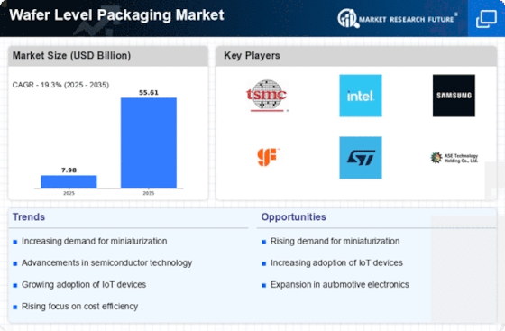
As per Market Research Future analysis, the Wafer Level Packaging Market was estimated at 8.6 USD Billion in 2024. The Wafer Level Packaging industry is projected to grow from 9.5 USD Billion in 2025 to 25.2 USD Billion by 2035, exhibiting a compound annual growth rate (CAGR) of 10.25% during the forecast period 2025 - 2035
Key Market Trends & Highlights
The Wafer Level Packaging Market is poised for substantial growth driven by technological advancements and increasing demand for miniaturized electronics.
- The market is witnessing a trend towards the miniaturization of electronic devices, enhancing portability and functionality.
- Sustainability initiatives are gaining traction, prompting manufacturers to adopt eco-friendly materials and processes.
- Integration with IoT technologies is becoming prevalent, facilitating smarter and more connected devices.
- Rising demand for high-performance electronics and advancements in semiconductor technology are key drivers propelling market growth.
Market Size & Forecast
| 2024 Market Size | 8.6 (USD Billion) |
| 2035 Market Size | 25.2 (USD Billion) |
| CAGR (2025 - 2035) | 10.25% |
Major Players
TSMC (TW), Intel (US), Samsung (KR), GlobalFoundries (US), STMicroelectronics (FR), ASE Technology Holding Co., Ltd. (TW), Amkor Technology (US), Siliconware Precision Industries Co., Ltd. (TW), NXP Semiconductors (NL)

