Segmentation Quick Reference
| Dimension | Sub-Segments | Dominant Segment (2025) | Fastest Growing Segment (2026–2035) |
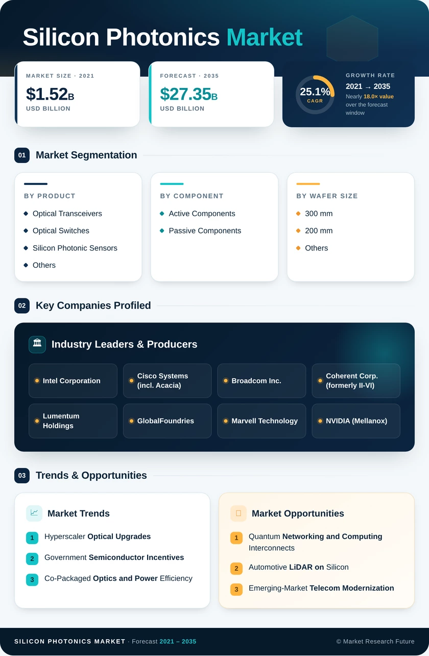
| Product | Optical Transceivers, Optical Switches, Silicon Photonic Sensors, Others | Optical Transceivers (51.2 % share) | Silicon Photonic Sensors (26.5 % CAGR) |
| Component | Active Components, Passive Components | Active Components (63.1 % share) | Active Components |
| Wafer Size | 300 mm, 200 mm, Others | 300 mm | 300 mm (25.6 % CAGR) |
| Data Rate | 200 Gbps, 400 Gbps, Above 1.6 Tbps | 400 Gbps (49.2 % share) | Above 1.6 Tbps (26.0 % CAGR) |
| Application | Data Centers & HPC, Telecommunications, Quantum Computing, Others | Data Centers & HPC (51.4 % share) | Quantum Computing (26.6 % CAGR) |
| End User | Hyperscale Silicon Photonics Market Providers, Telecom Operators, Automotive OEMs & Tier-1 Suppliers, Others | Hyperscale Silicon Photonics Market Providers (54.1 % share) | Automotive OEMs & Tier-1 Suppliers (26.2 % CAGR) |
Market Segmentation Overview
By Product
| Sub-Segment | Key Trend |
| Optical Transceivers | Migration from 400G to 800G and 1.6T form factors for hyperscale deployment |
| Optical Switches | Growth in reconfigurable optical add-drop multiplexer (ROADM) mesh architectures |
| Silicon Photonic Sensors | Expansion into automotive LiDAR, biomedical point-of-care, and environmental monitoring |
| Others | Specialty couplers, attenuators, and polarization-management devices for niche applications |
Optical transceivers drive the majority of silicon photonics revenue today, with the technology roadmap progressing toward higher lane rates and co-packaged form factors that integrate optics directly onto switch ASICs.
By Component
| Sub-Segment | Key Trend |
| Active Components | Higher-speed modulators and germanium photodetectors for 800G and 1.6T links |
| Passive Components | Low-loss waveguides and arrayed waveguide gratings for on-chip WDM |
Active components command the larger share because they define the performance envelope of every transceiver and sensor module, while passive structures serve as routing and multiplexing infrastructure.
By Wafer Size
| Sub-Segment | Key Trend |
| 300 mm | CHIPS Act–funded fab build-out enabling high-volume, low-cost production |
| 200 mm | Legacy node serving mature products and specialty sensors |
| Others | Emerging exploration of non-standard substrates for heterogeneous integration |
The 300 mm node is the primary growth vector, offering roughly 2.25× the die area per wafer versus 200 mm platforms and enabling significant cost-per-device reduction.
By Data Rate
| Sub-Segment | Key Trend |
| 200 Gbps | Steady demand from enterprise campus and edge deployments |
| 400 Gbps | Current mainstream hyperscaler standard with broad supply chain maturity |
| Above 1.6 Tbps | Emerging specification driven by AI training cluster bandwidth requirements |
The data-rate mix is shifting rapidly upward as each new generation of GPU clusters demands higher aggregate bandwidth per switch, compressing pluggable-to-co-packaged transition timelines.
By Application
| Sub-Segment | Key Trend |
| Data Centers & HPC | Dominant use case fueled by AI/ML workload scaling |
| Telecommunications | Metro and long-haul coherent links transitioning to silicon photonics PICs |
| Quantum Computing | Photonic interconnects for qubit control and entanglement distribution |
| Others | Defense, industrial sensing, and biomedical diagnostics |
Data center and HPC applications absorb the majority of silicon photonics output, with telecom and quantum computing representing the highest incremental growth vectors through 2035.
By End User
| Sub-Segment | Key Trend |
| Hyperscale Silicon Photonics Market Providers | Largest buyer cohort driving technology roadmap and volume pricing |
| Telecom Operators | Network disaggregation creating demand for open, interoperable photonic modules |
| Automotive OEMs & Tier-1 Suppliers | LiDAR and in-vehicle sensing adoption accelerating in ADAS and autonomy |
| Others | Government, research institutions, and defense contractors |
Hyperscale cloud providers set the pace for silicon photonics innovation through direct engagement with foundries and design houses, while automotive represents the highest-growth opportunity as silicon photonics enables affordable solid-state LiDAR at mass-market scale.