×
Hero Background
English
Chinese
French
Japanese
Korean
German
Spanish

Wafer Level Packaging Market Size

ID: MRFR/SEM/10774-HCR
128 Pages
Snehal Singh
October 2025

Wafer Level Packaging Market Research Report Information By Type (3D TSV WLP, 2.5D TSV WLP, WLCSP, Nano WLP and Others), By Technology (Fan in wafer level packaging and Fan out wafer level packaging), By End-User (Consumer Electronics, IT and Telecommunication, Automotive and Healthcare), and By Region (North America, Europe, Asia-Pacific, And Rest Of The World) –Industry Forecast Till 2035

Share:
Download PDF ×

We do not share your information with anyone. However, we may send you emails based on your report interest from time to time. You may contact us at any time to opt-out.

Wafer Level Packaging Market Infographic
Purchase Options

Wafer Level Packaging Size

Wafer Level Packaging Market Growth Projections and Opportunities

WLP's market for wafer back-end production and other related products is constantly under numerous kinds of impetus, with various factors defining the direction of it all; this affects demand, technology development and semiconductor industry growth. Wafer-level packaging is closely linked to the miniaturization trend sweeping across electronics. With electronic devices getting increasingly smaller and more compact, even higher-level packaging technologies such as wafer level packaging are required to keep up with the changing form factors. Connecting a number of functions and components in one semiconductor package is an important force behind wafer-level packaging. Selecting an interlayer spacing based on these considerations is one way to glean the best performance out of a chip. It also allows for shorter lengths in wiring connections and greater speed throughout electronic devices, thereby increasing efficiency overall. Portable and wearable electronic devices, from smartphones to IoT (Internet of Things) are increasingly popular in the market. So wafer-level packaging is also stimulated by greater demand for these applications. Because these applications require compact and lightweight packages, WLP is essential to semiconductor manufacturers. The development and adoption of wafer-level packaging is also influenced by advances in semiconductor manufacturing technologies such as advanced lithography, improved materials. Innovative manufacturing processes also help to make WLP solutions scalable and cost effective. The arrival of 5G boosts the need for high-performance semiconductors with greater processing speeds. Whether in 5G applications or elsewhere, performance requirements are very demanding. Wafer-level packaging can improve signal integrity and reduce parasitic effects. The demand for interconnection between networked devices and the proliferation of Internet of Things (IoT) applications fuel this market. WLP can produce compact, low-energy consuming semiconductor devices for a wide range of IoT applications from smart home products to industrial sensors. However, fan-out wafer-level packaging (FO-WLP) is a great step forward in the market. Increased flexibility in placing semiconductor components, better heat dissipation and electrical characteristics: these are reasons why fo-wlp is increasingly gaining importance for high performance applications. As the automotive industry's use of electronics and semiconductor components continues to increase, demand for wafer-level packaging also grows. WLP solutions are designed to satisfy the demanding needs of automotive applications: dependability, miniaturization and long service life in extreme conditions. As environmental issues and regulations affect the wafer-level packaging market, customers progressively turn to lead-free packaging solutions. In choosing materials and manufacturing processes, manufacturers and end-users are both looking for environmentally friendly packaging solutions. Design and packaging trends in the global semiconductor industry, among other factors such as mergers and acquisitions or technological alliances, form a competitive environment for wafer-level packaging. These include strategic collaborations and industry developments that affect market dynamics.
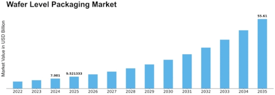
Wafer Level Packaging Market Size Graph
Author
Snehal Singh
Assistant Manager - Research

High acumen in analyzing complex macro & micro markets with more than 6 years of work experience in the field of market research. By implementing her analytical skills in forecasting and estimation into market research reports, she has expertise in Packaging, Construction, and Equipment domains. She handles a team size of 20-25 resources and ensures smooth running of the projects, associated marketing activities, and client servicing.

Leave a Comment

FAQs

What is the projected market valuation of the Wafer Level Packaging Market by 2035?

<p>The Wafer Level Packaging Market is projected to reach a valuation of 55.61 USD Billion by 2035.</p>

What was the market valuation of the Wafer Level Packaging Market in 2024?

<p>In 2024, the Wafer Level Packaging Market was valued at 7.981 USD Billion.</p>

What is the expected CAGR for the Wafer Level Packaging Market during the forecast period 2025 - 2035?

<p>The expected CAGR for the Wafer Level Packaging Market during the forecast period 2025 - 2035 is 19.3%.</p>

Which companies are considered key players in the Wafer Level Packaging Market?

<p>Key players in the Wafer Level Packaging Market include TSMC, Intel, Samsung, GlobalFoundries, and others.</p>

What are the main types of Wafer Level Packaging and their projected valuations?

<p>The main types include 3D TSV WLP, 2.5D TSV WLP, WLCSP, Nano WLP, and others, with valuations ranging from 1.0 to 15.0 USD Billion.</p>

How does the Fan Out Wafer Level Packaging segment compare to Fan In Wafer Level Packaging in terms of market size?

<p>Fan Out Wafer Level Packaging is projected to reach 37.12 USD Billion, while Fan In Wafer Level Packaging is expected to reach 18.5 USD Billion.</p>

Market Summary

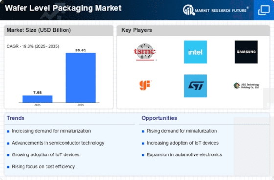
As per MRFR analysis, the Wafer Level Packaging Market was estimated at 7.981 USD Billion in 2024. The Wafer Level Packaging industry is projected to grow from 9.521 USD Billion in 2025 to 55.61 USD Billion by 2035, exhibiting a compound annual growth rate (CAGR) of 19.3 during the forecast period 2025 - 2035.

Key Market Trends & Highlights

The Wafer Level Packaging Market is poised for substantial growth driven by technological advancements and increasing demand for miniaturized electronics.

  • The market is witnessing a trend towards the miniaturization of electronic devices, enhancing portability and functionality. Sustainability initiatives are gaining traction, prompting manufacturers to adopt eco-friendly materials and processes. Integration with IoT technologies is becoming prevalent, facilitating smarter and more connected devices. Rising demand for high-performance electronics and advancements in semiconductor technology are key drivers propelling market growth.

Market Size & Forecast

2024 Market Size 7.981 (USD Billion)
2035 Market Size 55.61 (USD Billion)
CAGR (2025 - 2035) 19.3%
Largest Regional Market Share in 2024 North America

Major Players

<p>TSMC (TW), Intel (US), Samsung (KR), GlobalFoundries (US), STMicroelectronics (FR), ASE Technology Holding Co., Ltd. (TW), Amkor Technology (US), Siliconware Precision Industries Co., Ltd. (TW), NXP Semiconductors (NL)</p>

Market Trends

The Wafer Level Packaging Market is currently experiencing a transformative phase, driven by advancements in semiconductor technology and the increasing demand for miniaturized electronic devices. This market appears to be expanding as manufacturers seek to enhance performance while reducing the size and weight of components. The integration of wafer level packaging techniques allows for improved thermal management and electrical performance, which seems to be appealing to various sectors, including consumer electronics, automotive, and telecommunications. Furthermore, the trend towards Internet of Things (IoT) devices is likely to propel the adoption of wafer level packaging solutions, as these applications require compact and efficient packaging methods. In addition, the Wafer Level Packaging Market is witnessing a shift towards sustainable practices. Companies are increasingly focusing on environmentally friendly materials and processes, which may contribute to a more sustainable supply chain. This shift not only addresses regulatory pressures but also aligns with consumer preferences for greener products. As the market evolves, it appears that innovation in packaging technologies will play a crucial role in meeting the diverse needs of end-users, ultimately shaping the future landscape of the semiconductor industry. The ongoing research and development efforts indicate a promising outlook for wafer level packaging solutions in the coming years.

Miniaturization of Electronic Devices

The trend towards smaller and more efficient electronic devices is driving the demand for wafer level packaging solutions. As consumer electronics become increasingly compact, manufacturers are adopting advanced packaging techniques to meet these requirements.

Sustainability Initiatives

There is a growing emphasis on sustainable practices within the Wafer Level Packaging Market. Companies are exploring eco-friendly materials and processes, which may enhance their market appeal and comply with environmental regulations.

Integration with IoT Technologies

The rise of Internet of Things applications is influencing the Wafer Level Packaging Market. As IoT devices require efficient and compact packaging, this trend is likely to boost the adoption of innovative packaging solutions.

Wafer Level Packaging Market Market Drivers

Growing Adoption of 5G Technology

The rollout of 5G technology is poised to have a profound impact on the Wafer Level Packaging Market. With the increasing demand for faster data transmission and improved connectivity, there is a pressing need for advanced packaging solutions that can support the high-frequency requirements of 5G applications. Wafer level packaging offers the necessary performance characteristics, such as low inductance and reduced signal loss, making it suitable for 5G-enabled devices. The 5G infrastructure market is projected to reach approximately USD 700 billion by 2025, creating substantial opportunities for wafer level packaging providers. As telecommunications companies invest heavily in 5G networks, the demand for compatible packaging solutions is expected to rise, further driving the growth of the wafer level packaging market.

Increased Focus on Cost Efficiency

Cost efficiency remains a critical driver in the Wafer Level Packaging Market. As manufacturers seek to optimize production processes and reduce overall costs, wafer level packaging presents an attractive alternative to traditional packaging methods. The ability to integrate multiple functions into a single package not only minimizes material usage but also streamlines assembly processes. This efficiency can lead to significant cost savings, particularly in high-volume production scenarios. Reports suggest that companies utilizing wafer level packaging can achieve up to 30% reduction in manufacturing costs compared to conventional methods. As competition intensifies, the emphasis on cost-effective solutions is likely to drive further adoption of wafer level packaging technologies across various sectors, including consumer electronics and automotive.

Emergence of Automotive Electronics

The Wafer Level Packaging Market is witnessing a notable shift due to the emergence of automotive electronics. As vehicles become increasingly equipped with advanced electronic systems, the demand for reliable and efficient packaging solutions is on the rise. Wafer level packaging is particularly advantageous in automotive applications, where space constraints and performance reliability are critical. The automotive electronics market is anticipated to grow at a compound annual growth rate of around 7% through 2025, driven by trends such as electric vehicles and autonomous driving technologies. This growth presents a significant opportunity for wafer level packaging, as manufacturers seek to enhance the performance and reliability of automotive components. Consequently, the integration of wafer level packaging in automotive electronics is likely to become a key trend in the coming years.

Advancements in Semiconductor Technology

The Wafer Level Packaging Market is significantly influenced by advancements in semiconductor technology. As semiconductor manufacturers strive to enhance chip performance and reduce costs, wafer level packaging emerges as a viable solution. The integration of advanced materials and processes in wafer level packaging enables the production of smaller, more efficient chips. For instance, the introduction of 3D packaging techniques has the potential to increase chip density and performance, which is crucial for applications in artificial intelligence and machine learning. The semiconductor market is expected to grow at a compound annual growth rate of around 5.5% through 2025, further propelling the adoption of wafer level packaging solutions. This growth indicates a robust demand for innovative packaging technologies that can support the evolving needs of the semiconductor industry.

Rising Demand for High-Performance Electronics

The Wafer Level Packaging Market is experiencing a surge in demand for high-performance electronic devices. As consumer electronics evolve, there is a growing need for packaging solutions that can accommodate advanced functionalities while maintaining compact sizes. This trend is particularly evident in sectors blets, and wearables, where performance and miniaturization are paramount. The market for smartphones alone is projected to reach approximately 1.5 billion units by 2025, driving the need for innovative packaging solutions. Wafer level packaging offers a pathway to achieve these performance metrics, as it allows for reduced form factors and enhanced thermal management. Consequently, manufacturers are increasingly adopting wafer level packaging technologisuch as smartphones, taes to meet the expectations of consumers and maintain competitive advantages.

Market Segment Insights

Wafer Level Packaging Market Type Insights

<p>The wafer level packaging market segmentation, based on type includes 3D TSV WLP, 2.5D TSV WLP, WLCSP, Nano WLP and Others. The 2.5D TSV WLP segment dominated the market. The 2.5D TSV WLP is used widely because of its enhanced capacity, decreased system space requirements, improved performance, and low power consumption. In the years ahead, this factor would contribute to this segment's market-wide expansion being more rapid.</p>

Wafer Level Packaging Market Technology Insights

<p>The wafer level packaging market segmentation, based on technology, includes Fan in wafer level packaging and Fan out wafer level packaging. The fan in wafer level packaging category generated the most income. Fan-in WLP technology's dominance in the semiconductor industry, which provides indisputable advantages in terms of shape and cost, is credited with the segment's continued expansion. In addition, the variety of fan-in WLP systems keeps growing because to advancements in technology and innovation.</p>

<p>Source: Secondary Research, Primary Research, MRFR Database and Analyst Review</p>

Wafer Level Packaging Market End-User Insights

<p>The wafer level packaging market segmentation, based on end-user, includes Consumer Electronics, IT and Telecommunication, Automotive and Healthcare. The consumer electronics category generated the most income. The development of <a href="https://www.marketresearchfuture.com/reports/electronic-packaging-market-8705">electronic packaging </a>technology, which has led to the creation of extremely effective and reliable electrical connecting methods for electronic devices, is responsible for the segment's steady expansion.</p>

Get more detailed insights about Wafer Level Packaging Market Research Report - Global Forecast 2035

Regional Insights

North America : Innovation and Technology Hub

North America is the largest market for Wafer Level Packaging Market (WLP), holding approximately 40% of the global market share. The region's growth is driven by advancements in semiconductor technology, increasing demand for miniaturized electronic devices, and supportive government policies promoting innovation. The presence of major players like Intel and GlobalFoundries further fuels market expansion, alongside a robust ecosystem of research institutions and tech companies. The United States stands out as the leading country in this sector, with significant contributions from California and Texas. The competitive landscape is characterized by a mix of established firms and emerging startups, all vying for market share. Key players such as TSMC and Amkor Technology are investing heavily in R&D to enhance their WLP offerings, ensuring they remain at the forefront of technological advancements. The region's focus on sustainability and efficiency is also shaping future developments.

Europe : Emerging Market with Potential

Europe is witnessing a significant rise in the Wafer Level Packaging Market, currently holding around 25% of the global share. The growth is propelled by increasing demand for high-performance electronics and automotive applications, alongside stringent regulations promoting energy efficiency and sustainability. Countries like Germany and France are leading this growth, supported by government initiatives aimed at bolstering semiconductor manufacturing capabilities. Germany is the largest market in Europe, with a strong presence of key players such as STMicroelectronics and NXP Semiconductors. The competitive landscape is evolving, with collaborations between established firms and startups focusing on innovative packaging solutions. The European market is also characterized by a growing emphasis on research and development, driven by the need for advanced technologies in various sectors, including automotive and consumer electronics.

Asia-Pacific : Manufacturing Powerhouse

Asia-Pacific is a powerhouse in the Wafer Level Packaging Market, accounting for approximately 30% of the global share. The region's growth is fueled by the rapid expansion of consumer electronics, automotive, and telecommunications sectors. Countries like China, South Korea, and Taiwan are at the forefront, benefiting from strong manufacturing capabilities and government support for semiconductor innovation and production. China is the largest market in the region, with significant contributions from companies like TSMC and ASE Technology Holding. The competitive landscape is marked by intense rivalry among local and international players, all striving to enhance their WLP technologies. The region's focus on integrating advanced packaging solutions into next-generation devices is driving further investments and collaborations, ensuring its dominance in the global market.

Middle East and Africa : Emerging Frontier for Technology

The Middle East and Africa (MEA) region is emerging as a new frontier for the Wafer Level Packaging Market, currently holding about 5% of the global share. The growth is driven by increasing investments in technology infrastructure and a rising demand for electronic devices. Countries like South Africa and the UAE are making strides in developing their semiconductor industries, supported by government initiatives aimed at fostering innovation and attracting foreign investment. South Africa is leading the market in the region, with a growing number of tech startups and collaborations with international firms. The competitive landscape is still developing, with opportunities for both local and global players to establish a foothold. The region's focus on diversifying its economy and enhancing technological capabilities is expected to drive future growth in the Wafer Level Packaging Market sector.

Key Players and Competitive Insights

Leading market players are investing heavily in research and development in order to expand their product lines, which will help the wafer level packaging market, grow even more. Market participants are also undertaking a variety of strategic activities to expand their footprint, with important market developments including new product launches, contractual agreements, mergers and acquisitions, higher investments, and collaboration with other organizations. To expand and survive in a more competitive and rising market climate, wafer level packaging industry must offer cost-effective items.

Manufacturing locally to minimize operational costs is one of the key business tactics used by manufacturers in the wafer level packaging industry to benefit clients and increase the market sector. In recent years, the wafer level packaging industry has offered some of the most significant advantages to medicine. Major players in the wafer level packaging market are attempting to increase market demand by investing in research and development operations includes Fujitsu, Qualcomm Technologies, Inc., Tokyo Electron Ltd., Jiangsu Changjiang Electronics Technology Co. Ltd, Applied Materials, Inc., Amkor Technology, Inc., Lam Research Corporation, ASML Holding N.V, Toshiba Corporation, and Deca Technologies.

Amkor Technology Inc. (Amkor) offers solutions and services for semiconductor packaging and testing. The business provides complete system-level and final test services, as well as turnkey packaging and test services for semiconductor wafers, including bumping, back-grinding, packing, wafer probing, package design, and drop-shipping. It benefits contract foundries, original equipment manufacturers, integrated device makers (IDMs), and fabless semiconductor firms. The artificial intelligence, automotive, communications, computer, consumer, industrial, internet of things, and networking industries all find use for Amkor's products.

Offering equipment for semiconductor fabrication, ASML Holding NV (ASML) is a provider of microelectronics solutions. equipment for lithography, metrology and inspection, and remanufactured equipment are all part of the company's product line. The company's computational lithography and patterning control software solutions help clients achieve high yield and improved operating efficiency. The foundries, NAND-flash memory, and DRAM memory chip industries are all target markets for ASML's products.

Key Companies in the Wafer Level Packaging Market market include

Industry Developments

March 2023: For the networking and mobile sectors, ASE Inc. recently introduced its newly created advanced fan-out package-on-package (FoPoP) solutions. The company developed this technology to provide low latency and high bandwidth benefits for consumer electronics applications.

Future Outlook

Wafer Level Packaging Market Future Outlook

<p>The Wafer Level Packaging Market is projected to grow at a 19.3% CAGR from 2024 to 2035, driven by advancements in miniaturization, increased demand for consumer electronics, and the rise of IoT applications.</p>

New opportunities lie in:

  • <p>Development of advanced thermal management solutions for high-performance devices.</p>
  • <p>Expansion into emerging markets with tailored packaging solutions.</p>
  • <p>Investment in R&amp;D for next-generation materials to enhance performance.</p>

<p>By 2035, the Wafer Level Packaging Market is expected to achieve substantial growth, solidifying its critical role in the semiconductor industry.</p>

Market Segmentation

Wafer Level Packaging Market Type Outlook

  • 3D TSV WLP
  • 2.5D TSV WLP
  • WLCSP
  • Nano WLP
  • Others

Wafer Level Packaging Market End-User Outlook

  • Consumer Electronics
  • IT and Telecommunication
  • Automotive
  • Healthcare

Wafer Level Packaging Market Technology Outlook

  • Fan In Wafer Level Packaging
  • Fan Out Wafer Level Packaging

Report Scope

MARKET SIZE 2024 7.981(USD Billion)
MARKET SIZE 2025 9.521(USD Billion)
MARKET SIZE 2035 55.61(USD Billion)
COMPOUND ANNUAL GROWTH RATE (CAGR) 19.3% (2024 - 2035)
REPORT COVERAGE Revenue Forecast, Competitive Landscape, Growth Factors, and Trends
BASE YEAR 2024
Market Forecast Period 2025 - 2035
Historical Data 2019 - 2024
Market Forecast Units USD Billion
Key Companies Profiled Market analysis in progress
Segments Covered Market segmentation analysis in progress
Key Market Opportunities Advancements in miniaturization and integration drive growth in the Wafer Level Packaging Market.
Key Market Dynamics Technological advancements drive innovation in Wafer Level Packaging, enhancing performance and reducing manufacturing costs.
Countries Covered North America, Europe, APAC, South America, MEA

FAQs

What is the projected market valuation of the Wafer Level Packaging Market by 2035?

<p>The Wafer Level Packaging Market is projected to reach a valuation of 55.61 USD Billion by 2035.</p>

What was the market valuation of the Wafer Level Packaging Market in 2024?

<p>In 2024, the Wafer Level Packaging Market was valued at 7.981 USD Billion.</p>

What is the expected CAGR for the Wafer Level Packaging Market during the forecast period 2025 - 2035?

<p>The expected CAGR for the Wafer Level Packaging Market during the forecast period 2025 - 2035 is 19.3%.</p>

Which companies are considered key players in the Wafer Level Packaging Market?

<p>Key players in the Wafer Level Packaging Market include TSMC, Intel, Samsung, GlobalFoundries, and others.</p>

What are the main types of Wafer Level Packaging and their projected valuations?

<p>The main types include 3D TSV WLP, 2.5D TSV WLP, WLCSP, Nano WLP, and others, with valuations ranging from 1.0 to 15.0 USD Billion.</p>

How does the Fan Out Wafer Level Packaging segment compare to Fan In Wafer Level Packaging in terms of market size?

<p>Fan Out Wafer Level Packaging is projected to reach 37.12 USD Billion, while Fan In Wafer Level Packaging is expected to reach 18.5 USD Billion.</p>

  1. SECTION I: EXECUTIVE SUMMARY AND KEY HIGHLIGHTS
    1. EXECUTIVE SUMMARY
      1. Market Overview
      2. Key Findings
      3. Market Segmentation
      4. Competitive Landscape
      5. Challenges and Opportunities
      6. Future Outlook 2
  2. SECTION II: SCOPING, METHODOLOGY AND MARKET STRUCTURE
    1. MARKET INTRODUCTION
      1. Definition
      2. Scope of the study
    2. RESEARCH METHODOLOGY
      1. Overview
      2. Data Mining
      3. Secondary Research
      4. Primary Research
      5. Forecasting Model
      6. Market Size Estimation
      7. Data Triangulation
      8. Validation 3
  3. SECTION III: QUALITATIVE ANALYSIS
    1. MARKET DYNAMICS
      1. Overview
      2. Drivers
      3. Restraints
      4. Opportunities
    2. MARKET FACTOR ANALYSIS
      1. Value chain Analysis
      2. Porter's Five Forces Analysis
      3. COVID-19 Impact Analysis
  4. SECTION IV: QUANTITATIVE ANALYSIS
    1. Semiconductor & Electronics, BY Type (USD Billion)
      1. 3D TSV WLP
      2. WLCSP
      3. Nano WLP
      4. Others
    2. 2.5D TSV WLP
    3. Semiconductor & Electronics, BY Technology (USD Billion)
      1. Fan In Wafer Level Packaging
      2. Fan Out Wafer Level Packaging
    4. Semiconductor & Electronics, BY End-User (USD Billion)
      1. Consumer Electronics
      2. IT and Telecommunication
      3. Automotive
      4. Healthcare
    5. Semiconductor & Electronics, BY Region (USD Billion)
      1. North America
      2. Europe
      3. APAC
      4. South America
      5. MEA
  5. SECTION V: COMPETITIVE ANALYSIS
    1. Competitive Landscape
      1. Overview
      2. Competitive Analysis
      3. Market share Analysis
      4. Major Growth Strategy in the Semiconductor & Electronics
      5. Competitive Benchmarking
      6. Leading Players in Terms of Number of Developments in the Semiconductor & Electronics
      7. Key developments and growth strategies
      8. Major Players Financial Matrix
    2. Company Profiles
      1. TSMC (TW)
      2. Intel (US)
      3. Samsung (KR)
      4. GlobalFoundries (US)
      5. STMicroelectronics (FR)
      6. ASE Technology Holding Co., Ltd. (TW)
      7. Amkor Technology (US)
      8. Siliconware Precision Industries Co., Ltd. (TW)
      9. NXP Semiconductors (NL)
    3. Appendix
      1. References
      2. Related Reports 6 LIST OF FIGURES
    4. MARKET SYNOPSIS
    5. NORTH AMERICA MARKET ANALYSIS
    6. US MARKET ANALYSIS BY TYPE
    7. US MARKET ANALYSIS BY TECHNOLOGY
    8. US MARKET ANALYSIS BY END-USER
    9. CANADA MARKET ANALYSIS BY TYPE
    10. CANADA MARKET ANALYSIS BY TECHNOLOGY
    11. CANADA MARKET ANALYSIS BY END-USER
    12. EUROPE MARKET ANALYSIS
    13. GERMANY MARKET ANALYSIS BY TYPE
    14. GERMANY MARKET ANALYSIS BY TECHNOLOGY
    15. GERMANY MARKET ANALYSIS BY END-USER
    16. UK MARKET ANALYSIS BY TYPE
    17. UK MARKET ANALYSIS BY TECHNOLOGY
    18. UK MARKET ANALYSIS BY END-USER
    19. FRANCE MARKET ANALYSIS BY TYPE
    20. FRANCE MARKET ANALYSIS BY TECHNOLOGY
    21. FRANCE MARKET ANALYSIS BY END-USER
    22. RUSSIA MARKET ANALYSIS BY TYPE
    23. RUSSIA MARKET ANALYSIS BY TECHNOLOGY
    24. RUSSIA MARKET ANALYSIS BY END-USER
    25. ITALY MARKET ANALYSIS BY TYPE
    26. ITALY MARKET ANALYSIS BY TECHNOLOGY
    27. ITALY MARKET ANALYSIS BY END-USER
    28. SPAIN MARKET ANALYSIS BY TYPE
    29. SPAIN MARKET ANALYSIS BY TECHNOLOGY
    30. SPAIN MARKET ANALYSIS BY END-USER
    31. REST OF EUROPE MARKET ANALYSIS BY TYPE
    32. REST OF EUROPE MARKET ANALYSIS BY TECHNOLOGY
    33. REST OF EUROPE MARKET ANALYSIS BY END-USER
    34. APAC MARKET ANALYSIS
    35. CHINA MARKET ANALYSIS BY TYPE
    36. CHINA MARKET ANALYSIS BY TECHNOLOGY
    37. CHINA MARKET ANALYSIS BY END-USER
    38. INDIA MARKET ANALYSIS BY TYPE
    39. INDIA MARKET ANALYSIS BY TECHNOLOGY
    40. INDIA MARKET ANALYSIS BY END-USER
    41. JAPAN MARKET ANALYSIS BY TYPE
    42. JAPAN MARKET ANALYSIS BY TECHNOLOGY
    43. JAPAN MARKET ANALYSIS BY END-USER
    44. SOUTH KOREA MARKET ANALYSIS BY TYPE
    45. SOUTH KOREA MARKET ANALYSIS BY TECHNOLOGY
    46. SOUTH KOREA MARKET ANALYSIS BY END-USER
    47. MALAYSIA MARKET ANALYSIS BY TYPE
    48. MALAYSIA MARKET ANALYSIS BY TECHNOLOGY
    49. MALAYSIA MARKET ANALYSIS BY END-USER
    50. THAILAND MARKET ANALYSIS BY TYPE
    51. THAILAND MARKET ANALYSIS BY TECHNOLOGY
    52. THAILAND MARKET ANALYSIS BY END-USER
    53. INDONESIA MARKET ANALYSIS BY TYPE
    54. INDONESIA MARKET ANALYSIS BY TECHNOLOGY
    55. INDONESIA MARKET ANALYSIS BY END-USER
    56. REST OF APAC MARKET ANALYSIS BY TYPE
    57. REST OF APAC MARKET ANALYSIS BY TECHNOLOGY
    58. REST OF APAC MARKET ANALYSIS BY END-USER
    59. SOUTH AMERICA MARKET ANALYSIS
    60. BRAZIL MARKET ANALYSIS BY TYPE
    61. BRAZIL MARKET ANALYSIS BY TECHNOLOGY
    62. BRAZIL MARKET ANALYSIS BY END-USER
    63. MEXICO MARKET ANALYSIS BY TYPE
    64. MEXICO MARKET ANALYSIS BY TECHNOLOGY
    65. MEXICO MARKET ANALYSIS BY END-USER
    66. ARGENTINA MARKET ANALYSIS BY TYPE
    67. ARGENTINA MARKET ANALYSIS BY TECHNOLOGY
    68. ARGENTINA MARKET ANALYSIS BY END-USER
    69. REST OF SOUTH AMERICA MARKET ANALYSIS BY TYPE
    70. REST OF SOUTH AMERICA MARKET ANALYSIS BY TECHNOLOGY
    71. REST OF SOUTH AMERICA MARKET ANALYSIS BY END-USER
    72. MEA MARKET ANALYSIS
    73. GCC COUNTRIES MARKET ANALYSIS BY TYPE
    74. GCC COUNTRIES MARKET ANALYSIS BY TECHNOLOGY
    75. GCC COUNTRIES MARKET ANALYSIS BY END-USER
    76. SOUTH AFRICA MARKET ANALYSIS BY TYPE
    77. SOUTH AFRICA MARKET ANALYSIS BY TECHNOLOGY
    78. SOUTH AFRICA MARKET ANALYSIS BY END-USER
    79. REST OF MEA MARKET ANALYSIS BY TYPE
    80. REST OF MEA MARKET ANALYSIS BY TECHNOLOGY
    81. REST OF MEA MARKET ANALYSIS BY END-USER
    82. KEY BUYING CRITERIA OF SEMICONDUCTOR & ELECTRONICS
    83. RESEARCH PROCESS OF MRFR
    84. DRO ANALYSIS OF SEMICONDUCTOR & ELECTRONICS
    85. DRIVERS IMPACT ANALYSIS: SEMICONDUCTOR & ELECTRONICS
    86. RESTRAINTS IMPACT ANALYSIS: SEMICONDUCTOR & ELECTRONICS
    87. SUPPLY / VALUE CHAIN: SEMICONDUCTOR & ELECTRONICS
    88. SEMICONDUCTOR & ELECTRONICS, BY TYPE, 2024 (% SHARE)
    89. SEMICONDUCTOR & ELECTRONICS, BY TYPE, 2024 TO 2035 (USD Billion)
    90. SEMICONDUCTOR & ELECTRONICS, BY TECHNOLOGY, 2024 (% SHARE)
    91. SEMICONDUCTOR & ELECTRONICS, BY TECHNOLOGY, 2024 TO 2035 (USD Billion)
    92. SEMICONDUCTOR & ELECTRONICS, BY END-USER, 2024 (% SHARE)
    93. SEMICONDUCTOR & ELECTRONICS, BY END-USER, 2024 TO 2035 (USD Billion)
    94. BENCHMARKING OF MAJOR COMPETITORS 7 LIST OF TABLES
    95. LIST OF ASSUMPTIONS
    96. North America MARKET SIZE ESTIMATES; FORECAST
      1. BY TYPE, 2025-2035 (USD Billion)
      2. BY TECHNOLOGY, 2025-2035 (USD Billion)
      3. BY END-USER, 2025-2035 (USD Billion)
    97. US MARKET SIZE ESTIMATES; FORECAST
      1. BY TYPE, 2025-2035 (USD Billion)
      2. BY TECHNOLOGY, 2025-2035 (USD Billion)
      3. BY END-USER, 2025-2035 (USD Billion)
    98. Canada MARKET SIZE ESTIMATES; FORECAST
      1. BY TYPE, 2025-2035 (USD Billion)
      2. BY TECHNOLOGY, 2025-2035 (USD Billion)
      3. BY END-USER, 2025-2035 (USD Billion)
    99. Europe MARKET SIZE ESTIMATES; FORECAST
      1. BY TYPE, 2025-2035 (USD Billion)
      2. BY TECHNOLOGY, 2025-2035 (USD Billion)
      3. BY END-USER, 2025-2035 (USD Billion)
    100. Germany MARKET SIZE ESTIMATES; FORECAST
      1. BY TYPE, 2025-2035 (USD Billion)
      2. BY TECHNOLOGY, 2025-2035 (USD Billion)
      3. BY END-USER, 2025-2035 (USD Billion)
    101. UK MARKET SIZE ESTIMATES; FORECAST
      1. BY TYPE, 2025-2035 (USD Billion)
      2. BY TECHNOLOGY, 2025-2035 (USD Billion)
      3. BY END-USER, 2025-2035 (USD Billion)
    102. France MARKET SIZE ESTIMATES; FORECAST
      1. BY TYPE, 2025-2035 (USD Billion)
      2. BY TECHNOLOGY, 2025-2035 (USD Billion)
      3. BY END-USER, 2025-2035 (USD Billion)
    103. Russia MARKET SIZE ESTIMATES; FORECAST
      1. BY TYPE, 2025-2035 (USD Billion)
      2. BY TECHNOLOGY, 2025-2035 (USD Billion)
      3. BY END-USER, 2025-2035 (USD Billion)
    104. Italy MARKET SIZE ESTIMATES; FORECAST
      1. BY TYPE, 2025-2035 (USD Billion)
      2. BY TECHNOLOGY, 2025-2035 (USD Billion)
      3. BY END-USER, 2025-2035 (USD Billion)
    105. Spain MARKET SIZE ESTIMATES; FORECAST
      1. BY TYPE, 2025-2035 (USD Billion)
      2. BY TECHNOLOGY, 2025-2035 (USD Billion)
      3. BY END-USER, 2025-2035 (USD Billion)
    106. Rest of Europe MARKET SIZE ESTIMATES; FORECAST
      1. BY TYPE, 2025-2035 (USD Billion)
      2. BY TECHNOLOGY, 2025-2035 (USD Billion)
      3. BY END-USER, 2025-2035 (USD Billion)
    107. APAC MARKET SIZE ESTIMATES; FORECAST
      1. BY TYPE, 2025-2035 (USD Billion)
      2. BY TECHNOLOGY, 2025-2035 (USD Billion)
      3. BY END-USER, 2025-2035 (USD Billion)
    108. China MARKET SIZE ESTIMATES; FORECAST
      1. BY TYPE, 2025-2035 (USD Billion)
      2. BY TECHNOLOGY, 2025-2035 (USD Billion)
      3. BY END-USER, 2025-2035 (USD Billion)
    109. India MARKET SIZE ESTIMATES; FORECAST
      1. BY TYPE, 2025-2035 (USD Billion)
      2. BY TECHNOLOGY, 2025-2035 (USD Billion)
      3. BY END-USER, 2025-2035 (USD Billion)
    110. Japan MARKET SIZE ESTIMATES; FORECAST
      1. BY TYPE, 2025-2035 (USD Billion)
      2. BY TECHNOLOGY, 2025-2035 (USD Billion)
      3. BY END-USER, 2025-2035 (USD Billion)
    111. South Korea MARKET SIZE ESTIMATES; FORECAST
      1. BY TYPE, 2025-2035 (USD Billion)
      2. BY TECHNOLOGY, 2025-2035 (USD Billion)
      3. BY END-USER, 2025-2035 (USD Billion)
    112. Malaysia MARKET SIZE ESTIMATES; FORECAST
      1. BY TYPE, 2025-2035 (USD Billion)
      2. BY TECHNOLOGY, 2025-2035 (USD Billion)
      3. BY END-USER, 2025-2035 (USD Billion)
    113. Thailand MARKET SIZE ESTIMATES; FORECAST
      1. BY TYPE, 2025-2035 (USD Billion)
      2. BY TECHNOLOGY, 2025-2035 (USD Billion)
      3. BY END-USER, 2025-2035 (USD Billion)
    114. Indonesia MARKET SIZE ESTIMATES; FORECAST
      1. BY TYPE, 2025-2035 (USD Billion)
      2. BY TECHNOLOGY, 2025-2035 (USD Billion)
      3. BY END-USER, 2025-2035 (USD Billion)
    115. Rest of APAC MARKET SIZE ESTIMATES; FORECAST
      1. BY TYPE, 2025-2035 (USD Billion)
      2. BY TECHNOLOGY, 2025-2035 (USD Billion)
      3. BY END-USER, 2025-2035 (USD Billion)
    116. South America MARKET SIZE ESTIMATES; FORECAST
      1. BY TYPE, 2025-2035 (USD Billion)
      2. BY TECHNOLOGY, 2025-2035 (USD Billion)
      3. BY END-USER, 2025-2035 (USD Billion)
    117. Brazil MARKET SIZE ESTIMATES; FORECAST
      1. BY TYPE, 2025-2035 (USD Billion)
      2. BY TECHNOLOGY, 2025-2035 (USD Billion)
      3. BY END-USER, 2025-2035 (USD Billion)
    118. Mexico MARKET SIZE ESTIMATES; FORECAST
      1. BY TYPE, 2025-2035 (USD Billion)
      2. BY TECHNOLOGY, 2025-2035 (USD Billion)
      3. BY END-USER, 2025-2035 (USD Billion)
    119. Argentina MARKET SIZE ESTIMATES; FORECAST
      1. BY TYPE, 2025-2035 (USD Billion)
      2. BY TECHNOLOGY, 2025-2035 (USD Billion)
      3. BY END-USER, 2025-2035 (USD Billion)
    120. Rest of South America MARKET SIZE ESTIMATES; FORECAST
      1. BY TYPE, 2025-2035 (USD Billion)
      2. BY TECHNOLOGY, 2025-2035 (USD Billion)
      3. BY END-USER, 2025-2035 (USD Billion)
    121. MEA MARKET SIZE ESTIMATES; FORECAST
      1. BY TYPE, 2025-2035 (USD Billion)
      2. BY TECHNOLOGY, 2025-2035 (USD Billion)
      3. BY END-USER, 2025-2035 (USD Billion)
    122. GCC Countries MARKET SIZE ESTIMATES; FORECAST
      1. BY TYPE, 2025-2035 (USD Billion)
      2. BY TECHNOLOGY, 2025-2035 (USD Billion)
      3. BY END-USER, 2025-2035 (USD Billion)
    123. South Africa MARKET SIZE ESTIMATES; FORECAST
      1. BY TYPE, 2025-2035 (USD Billion)
      2. BY TECHNOLOGY, 2025-2035 (USD Billion)
      3. BY END-USER, 2025-2035 (USD Billion)
    124. Rest of MEA MARKET SIZE ESTIMATES; FORECAST
      1. BY TYPE, 2025-2035 (USD Billion)
      2. BY TECHNOLOGY, 2025-2035 (USD Billion)
      3. BY END-USER, 2025-2035 (USD Billion)
    125. PRODUCT LAUNCH/PRODUCT DEVELOPMENT/APPROVAL
    126. ACQUISITION/PARTNERSHIP

Wafer Level Packaging Market Segmentation

Wafer Level Packaging Type Outlook (USD Billion, 2020-2034)

  • 3D TSV WLP
  • 2.5D TSV WLP
  • WLCSP
  • Nano WLP
  • Others

Wafer Level Packaging Technology Outlook (USD Billion, 2020-2034)

  • Fan In Wafer Level Packaging
  • Fan Out Wafer Level Packaging

Wafer Level Packaging End-User Outlook (USD Billion, 2020-2034)

  • Consumer Electronics
  • IT and Telecommunication
  • Automotive
  • Healthcare

Wafer Level Packaging Regional Outlook (USD Billion, 2020-2034)

  • North America Outlook (USD Billion, 2020-2034)
    • North America Wafer Level Packaging by Type
      • 3D TSV WLP
      • 2.5D TSV WLP
      • WLCSP
      • Nano WLP
  • Others
  • North America Wafer Level Packaging by Technology
    • Fan In Wafer Level Packaging
    • Fan Out Wafer Level Packaging
  • North America Wafer Level Packaging by End-User
    • Consumer Electronics
    • IT and Telecommunication
    • Automotive
    • Healthcare
  • US Outlook (USD Billion, 2020-2034)
  • US Wafer Level Packaging by Type
    • 3D TSV WLP
    • 2.5D TSV WLP
    • WLCSP
    • Nano WLP
    • Others
  • US Wafer Level Packaging by Technology
    • Fan In Wafer Level Packaging
    • Fan Out Wafer Level Packaging
  • US Wafer Level Packaging by End-User
    • Consumer Electronics
    • IT and Telecommunication
    • Automotive
    • Healthcare
  • Canada Outlook (USD Billion, 2020-2034)
  • Canada Wafer Level Packaging by Type
    • 3D TSV WLP
    • 2.5D TSV WLP
    • WLCSP
    • Nano WLP
    • Others
  • Canada Wafer Level Packaging by Technology
    • Fan In Wafer Level Packaging
    • Fan Out Wafer Level Packaging
  • Canada Wafer Level Packaging by End-User
    • Consumer Electronics
    • IT and Telecommunication
    • Automotive
    • Healthcare
  • Europe Outlook (USD Billion, 2020-2034)
    • Europe Wafer Level Packaging by Type
      • 3D TSV WLP
      • 2.5D TSV WLP
      • WLCSP
      • Nano WLP
      • Others
    • Europe Wafer Level Packaging by Technology
      • Fan In Wafer Level Packaging
      • Fan Out Wafer Level Packaging
    • Europe Wafer Level Packaging by End-User
      • Consumer Electronics
      • IT and Telecommunication
      • Automotive
      • Healthcare
    • Germany Outlook (USD Billion, 2020-2034)
    • Germany Wafer Level Packaging by Type
      • 3D TSV WLP
      • 2.5D TSV WLP
      • WLCSP
      • Nano WLP
      • Others
    • Germany Wafer Level Packaging by Technology
      • Fan In Wafer Level Packaging
      • Fan Out Wafer Level Packaging
    • Germany Wafer Level Packaging by End-User
      • Consumer Electronics
      • IT and Telecommunication
      • Automotive
      • Healthcare
    • France Outlook (USD Billion, 2020-2034)
    • France Wafer Level Packaging by Type
      • 3D TSV WLP
      • 2.5D TSV WLP
      • WLCSP
      • Nano WLP
  • Others
  • France Wafer Level Packaging by Technology
    • Fan In Wafer Level Packaging
    • Fan Out Wafer Level Packaging
  • France Wafer Level Packaging by End-User
    • Consumer Electronics
    • IT and Telecommunication
    • Automotive
    • Healthcare
  • UK Outlook (USD Billion, 2020-2034)
  • UK Wafer Level Packaging by Type
    • 3D TSV WLP
    • 2.5D TSV WLP
    • WLCSP
    • Nano WLP
    • Others
  • UK Wafer Level Packaging by Technology
    • Fan In Wafer Level Packaging
    • Fan Out Wafer Level Packaging
  • UK Wafer Level Packaging by End-User
    • Consumer Electronics
    • IT and Telecommunication
    • Automotive
    • Healthcare
  • Italy Outlook (USD Billion, 2020-2034)
  • Italy Wafer Level Packaging by Type
    • 3D TSV WLP
    • 2.5D TSV WLP
    • WLCSP
    • Nano WLP
    • Others
  • Italy Wafer Level Packaging by Technology
    • Fan In Wafer Level Packaging
    • Fan Out Wafer Level Packaging
  • Italy Wafer Level Packaging by End-User
    • Consumer Electronics
    • IT and Telecommunication
    • Automotive
    • Healthcare
  • Spain Outlook (USD Billion, 2020-2034)
  • Spain Wafer Level Packaging by Type
    • 3D TSV WLP
    • 2.5D TSV WLP
    • WLCSP
    • Nano WLP
    • Others
  • Spain Wafer Level Packaging by Technology
    • Fan In Wafer Level Packaging
    • Fan Out Wafer Level Packaging
  • Spain Wafer Level Packaging by End-User
    • Consumer Electronics
    • IT and Telecommunication
    • Automotive
    • Healthcare
  • Rest Of Europe Outlook (USD Billion, 2020-2034)
  • Rest Of Europe Wafer Level Packaging by Type
    • 3D TSV WLP
    • 2.5D TSV WLP
    • WLCSP
    • Nano WLP
    • Others
  • Rest Of Europe Wafer Level Packaging by Technology
    • Fan In Wafer Level Packaging
    • Fan Out Wafer Level Packaging
  • Rest Of Europe Wafer Level Packaging by End-User
    • Consumer Electronics
    • IT and Telecommunication
    • Automotive
    • Healthcare
  • Asia-Pacific Outlook (USD Billion, 2020-2034)
    • Asia-Pacific Wafer Level Packaging by Type
      • 3D TSV WLP
      • 2.5D TSV WLP
      • WLCSP
      • Nano WLP
      • Others
    • Asia-Pacific Wafer Level Packaging by Technology
      • Fan In Wafer Level Packaging
      • Fan Out Wafer Level Packaging
    • Asia-Pacific Wafer Level Packaging by End-User
      • Consumer Electronics
      • IT and Telecommunication
      • Automotive
      • Healthcare
    • China Outlook (USD Billion, 2020-2034)
    • China Wafer Level Packaging by Type
      • 3D TSV WLP
      • 2.5D TSV WLP
      • WLCSP
      • Nano WLP
      • Others
    • China Wafer Level Packaging by Technology
      • Fan In Wafer Level Packaging
      • Fan Out Wafer Level Packaging
    • China Wafer Level Packaging by End-User
      • Consumer Electronics
      • IT and Telecommunication
      • Automotive
      • Healthcare
    • Japan Outlook (USD Billion, 2020-2034)
    • Japan Wafer Level Packaging by Type
      • 3D TSV WLP
      • 2.5D TSV WLP
      • WLCSP
      • Nano WLP
      • Others
    • Japan Wafer Level Packaging by Technology
      • Fan In Wafer Level Packaging
      • Fan Out Wafer Level Packaging
    • Japan Wafer Level Packaging by End-User
      • Consumer Electronics
      • IT and Telecommunication
      • Automotive
      • Healthcare
    • India Outlook (USD Billion, 2020-2034)
    • India Wafer Level Packaging by Type
      • 3D TSV WLP
      • 2.5D TSV WLP
      • WLCSP
      • Nano WLP
      • Others
    • India Wafer Level Packaging by Technology
      • Fan In Wafer Level Packaging
      • Fan Out Wafer Level Packaging
    • India Wafer Level Packaging by End-User
      • Consumer Electronics
      • IT and Telecommunication
      • Automotive
      • Healthcare
    • Australia Outlook (USD Billion, 2020-2034)
    • Australia Wafer Level Packaging by Type
      • 3D TSV WLP
      • 2.5D TSV WLP
      • WLCSP
      • Nano WLP
      • Others
    • Australia Wafer Level Packaging by Technology
      • Fan In Wafer Level Packaging
      • Fan Out Wafer Level Packaging
    • Australia Wafer Level Packaging by End-User
      • Consumer Electronics
      • IT and Telecommunication
      • Automotive
      • Healthcare
    • Rest of Asia-Pacific Outlook (USD Billion, 2020-2034)
    • Rest of Asia-Pacific Wafer Level Packaging by Type
      • 3D TSV WLP
      • 2.5D TSV WLP
      • WLCSP
      • Nano WLP
      • Others
    • Rest of Asia-Pacific Wafer Level Packaging by Technology
      • Fan In Wafer Level Packaging
      • Fan Out Wafer Level Packaging
    • Rest of Asia-Pacific Wafer Level Packaging by End-User
      • Consumer Electronics
      • IT and Telecommunication
      • Automotive
      • Healthcare
  • Rest of the World Outlook (USD Billion, 2020-2034)
    • Rest of the World Wafer Level Packaging by Type
      • 3D TSV WLP
      • 2.5D TSV WLP
      • WLCSP
      • Nano WLP
      • Others
    • Rest of the World Wafer Level Packaging by Technology
      • Fan In Wafer Level Packaging
      • Fan Out Wafer Level Packaging
    • Rest of the World Wafer Level Packaging by End-User
      • Consumer Electronics
      • IT and Telecommunication
      • Automotive
      • Healthcare
    • Middle East Outlook (USD Billion, 2020-2034)
    • Middle East Wafer Level Packaging by Type
      • 3D TSV WLP
      • 2.5D TSV WLP
      • WLCSP
      • Nano WLP
      • Others
    • Middle East Wafer Level Packaging by Technology
      • Fan In Wafer Level Packaging
      • Fan Out Wafer Level Packaging
    • Middle East Wafer Level Packaging by End-User
      • Consumer Electronics
      • IT and Telecommunication
      • Automotive
      • Healthcare
    • Africa Outlook (USD Billion, 2020-2034)
    • Africa Wafer Level Packaging by Type
      • 3D TSV WLP
      • 2.5D TSV WLP
      • WLCSP
      • Nano WLP
      • Others
    • Africa Wafer Level Packaging by Technology
      • Fan In Wafer Level Packaging
      • Fan Out Wafer Level Packaging
    • Africa Wafer Level Packaging by End-User
      • Consumer Electronics
      • IT and Telecommunication
      • Automotive
      • Healthcare
    • Latin America Outlook (USD Billion, 2020-2034)
    • Latin America Wafer Level Packaging by Type
      • 3D TSV WLP
      • 2.5D TSV WLP
      • WLCSP
      • Nano WLP
      • Others
    • Latin America Wafer Level Packaging by Technology
      • Fan In Wafer Level Packaging
      • Fan Out Wafer Level Packaging
    • Latin America Wafer Level Packaging by End-User
      • Consumer Electronics
      • IT and Telecommunication
      • Automotive
      • Healthcare
Infographic

Free Sample Request

Kindly complete the form below to receive a free sample of this Report

Get Free Sample

Customer Strories

“I am very pleased with how market segments have been defined in a relevant way for my purposes (such as "Portable Freezers & refrigerators" and "last-mile"). In general the report is well structured. Thanks very much for your efforts.”

Victoria Milne

Founder

Compare Licence

×
Features License Type
Single User Multiuser License Enterprise User
Price $4,950 $5,950 $7,250
Maximum User Access Limit 1 User Upto 10 Users Unrestricted Access Throughout the Organization
Free Customization
Direct Access to Analyst
Deliverable Format
Platform Access
Discount on Next Purchase 10% 15% 15%
Printable Versions