Electron Microscope Market (2026 - 2035)

Electron Microscope Market Research Report: Size, Share, Trend Analysis By Types (Transmission Electron Microscope, Scanning Electron Microscope and Others), By Applications (Nanotechnology, Material Sciences, Semiconductors, and Others), And By Region (North America, Europe, Asia-Pacific, And Rest Of The World) - Growth Outlook & Industry Forecast 2025 To 2035
ID: MRFR/MED/5193-HCR
100 Pages
Rahul Gotadki, Kinjoll Dey
Last Updated: June 25, 2026
Electron Microscope Market
Market Size
Forecast Period2026-2035
CAGR (2026-2035)7.5%
2035 Market SizeUSD 10.80 Billion
Key Players
Thermo Fisher Scientific
JEOL Ltd.
Hitachi High-Tech Corporation
Carl Zeiss Microscopy
Tescan Group
Nikon Corporation
Opportunities
  • Benchtop and Compact SEM Democratization
  • Software-Defined Throughput and Data Monetization
  • Emerging-Market National Facility Build-Outs

Electron Microscope Market Summary

The Global Electron Microscope Market size was valued at USD 5.25 Billion in 2025, and the market is projected to grow from USD 5.64 Billion in 2026 to USD 10.80 Billion by 2035, registering a CAGR of 7.5% during the forecast period 2026–2035. Two forces are pulling this expansion forward: the global semiconductor industry's push toward sub-3nm gate-all-around transistor architectures — catalyzed by the USD 52.7 Billion CHIPS and Science Act in the United States [1] — and a parallel surge in cryo-electron microscopy installations across government-funded life-science campuses. The Electron Microscope Market sits at the intersection of advanced manufacturing and fundamental research, making it uniquely resistant to single-sector downturns.

A technology overhaul is redefining how laboratories and fabs acquire electron microscopy platforms. Legacy thermionic-source instruments are steadily giving way to cold field-emission and Schottky emitter systems capable of sub-angstrom resolution, while artificial-intelligence-driven automation now condenses cryo-EM data-collection runs from multi-day campaigns to overnight sessions. The European Commission committed EUR 13.5 Billion to its Chips Act implementation, and a meaningful share of that funding targets advanced metrology infrastructure, including transmission electron microscopy capabilities at pilot lines in Dresden and Leuven [2].

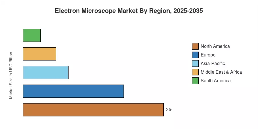
North America accounted for 38.2% of the Electron Microscope Market in 2025, anchored by semiconductor fabrication expansion in Arizona, Texas, and Ohio. Asia-Pacific stands as the fastest-growing region at a projected 12.4% CAGR through 2035, led by national electron-optics capacity programs in China and India. Europe holds the second-largest share at 27.5%, driven by automotive semiconductor demand and academic instrumentation renewal cycles. As national security concerns increasingly shape technology procurement, the Electron Microscope Market is poised for sustained geographic diversification through the decade.


Key Report Takeaways

• By Instrument Type

  • SEM platforms commanded a 72.5% share of the Electron Microscope Market in 2025, reflecting their dominance in high-throughput wafer inspection and routine biological screening workflows.
  • TEM instruments are forecast to grow at a 12.7% CAGR through 2035 as atomic-resolution defect localization becomes non-negotiable for advanced-node chip manufacturing.
  • Dual-beam FIB-SEM systems generated USD 0.38 Billion in 2025 revenue, driven by advanced packaging and failure-analysis demand.

• By Application

  • Life sciences and biology represented 22.8% of the Electron Microscope Market in 2025, with structural biology and vaccine research powering instrument procurement.
  • Nanotechnology applications are projected to expand at a 10.1% CAGR, fueled by nanoparticle characterization mandates in pharmaceuticals and energy storage.

• By Region

  • North America captured 38.2% of global spending in 2025, with the U.S. accounting for over three-quarters of regional revenue.
  • Asia-Pacific is forecast to grow at a 12.4% CAGR through 2035 as China and India invest in domestic electron-optics manufacturing.


Market Size and Forecast (2021–2035)

Market Research Future estimates are derived from a combination of bottom-up revenue modeling across instrument OEMs, top-down calibration using national science-funding databases, and triangulation with trade-flow data from customs authorities in major importing nations. Historical figures reflect actual shipment revenues; forecast values incorporate contracted pipeline visibility from leading manufacturers and announced government funding commitments.
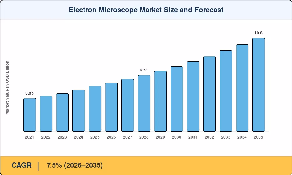
Electron Microscope Market Size and Forecast
Our Impact
Enabled $4.3B Revenue Impact for Fortune 500 and Leading Multinationals
Partnering with 2000+ Global Organizations Each Year
30K+ Citations by Top-Tier Firms in the Industry

Driver Impact Analysis

Driver ~% Impact on CAGR Geographic Relevance Impact Timeline
Sub-3nm semiconductor node transitions ~22% North America, Asia-Pacific Short-term (≤2 yr)
AI-automated cryo-EM workflows ~18% Global Medium-term (2–4 yr)
National electron-optics capacity programs ~15% China, India Medium-term (2–4 yr)
Battery gigafactory quality inspection ~14% Europe, North America Short-term (≤2 yr)
Correlative light-electron microscopy adoption ~10% Global Long-term (≥4 yr)
Structural biology & drug-discovery funding ~12% North America, Europe Medium-term (2–4 yr)
Advanced packaging & 3D chiplet architectures ~9% Asia-Pacific, North America Long-term (≥4 yr)


Sub-3nm Node Transitions and Fab Expansion

The semiconductor industry's migration to gate-all-around (GAA) transistor architectures at 3nm and below has made atomic-resolution metrology indispensable. TSMC's Arizona campus alone represents a USD 40 Billion investment, and each advanced-node fab typically requires 15–25 TEM and SEM platforms for inline defect review and process-development characterization [6]. Samsung and Intel are undertaking comparable buildouts, creating a procurement wave that directly benefits the Electron Microscope Market through 2028.

AI-Automated Cryo-EM Workflows

Machine-learning algorithms for automated particle picking and beam-tilt correction have compressed single-particle cryo-EM data collection from 72-hour campaigns to under 12 hours, boosting instrument utilization rates above 85% at leading structural-biology centers [8]. The NIH allocated USD 170 Million to national cryo-EM centers between 2023 and 2025, and the resulting throughput gains are encouraging pharmaceutical companies to bring cryo-EM screening in-house rather than rely on shared academic facilities [5].

National Electron-Optics Capacity Programs

China's 14th Five-Year Plan earmarked RMB 4.2 Billion for domestic precision-instrument development, explicitly targeting electron-optical column manufacturing to reduce dependency on Japanese and German suppliers [9]. India's Department of Science and Technology committed INR 1,800 Crore to the National Electron Microscopy Facility expansion. These programs are fragmenting a supply chain historically centered on three countries and opening procurement channels for the Electron Microscope Market across emerging economies.

Battery Gigafactory Quality Assurance

EV battery manufacturers now mandate cross-sectional SEM analysis of cathode and separator layers at every production lot. Europe alone has over 40 announced gigafactory projects expected online by 2030, each requiring dedicated materials-characterization labs [10]. The Electron Microscope Market benefits as these facilities procure benchtop and full-size SEM systems for quality-control workflows that did not exist at scale five years ago.


Restraints Impact Analysis

Restraint ~% Impact on CAGR Geographic Relevance Impact Timeline
High capital cost and total cost of ownership ~−18% Global (acute in emerging markets) Short-term (≤2 yr)
Export-control restrictions on electron optics ~−14% China, Russia Medium-term (2–4 yr)
Skilled operator shortage ~−12% Global Long-term (≥4 yr)
Long lead times for column assemblies ~−10% Global Short-term (≤2 yr)
Competition from alternative characterization tools ~−8% North America, Europe Long-term (≥4 yr)


Capital Cost and Total Cost of Ownership

A state-of-the-art aberration-corrected TEM can exceed USD 5 Million, and annual service contracts add 8–12% of the purchase price [13]. For universities in developing economies, this cost profile limits procurement to externally funded national facilities. The Electron Microscope Market faces a natural ceiling in price-sensitive segments until refurbished-instrument channels and lower-cost benchtop designs expand further.

Export-Control Restrictions

U.S. Bureau of Industry and Security rules and parallel Japanese export-licensing tightening have constrained shipments of advanced electron-optical columns to certain end users in China since late 2023 [14]. These controls slow Electron Microscope Market penetration in one of the world's fastest-growing R&D ecosystems and push Chinese institutions toward domestic suppliers whose performance lags by roughly one generation.

Skilled Operator Shortage

Operating a TEM at atomic resolution demands doctoral-level training, and the global supply of qualified microscopists has not kept pace with instrument installations. The Microscopy Society of America estimated a 30% shortfall in trained cryo-EM operators at U.S. national facilities in 2024 [15]. Until AI-assisted operation matures enough to de-skill routine sessions, human-capital constraints will moderate the pace at which new instruments translate into productive output.


Electron Microscope Market Opportunities

Benchtop and Compact SEM Democratization

Community colleges, mid-tier manufacturers’ quality-control laboratories, and emerging-market forensic agencies are finding that tabletop SEM platforms costing between USD 80,000 and USD 250,000 are opening procurement doors. This sector expanded over 14% YoY in 2024, and it provides a volume-driven channel for the Electron Microscope Market to reach buyers formerly priced out of floor-model equipment.


Software-Defined Throughput and Data Monetization

Instrument suppliers are moving toward subscription-based software modules — automated defect categorization, 3D tomography reconstruction and AI-driven specimen centering — that create recurring revenue streams beyond the original hardware sale. The shift to platform economics with software margins above 60% versus 25-30% for the hardware is evidenced by Thermo Fisher’s Athena platform and JEOL’s SightX suite.


Emerging-Market National Facility Build-Outs

India, Brazil and Saudi Arabia are establishing centralized electron microscopy centers related to national science initiatives. The projected 12-site network under the DST strategy and the KAUST growth in Saudi Arabia together generate addressable pockets for the Electron Microscope Market worth an estimated USD 400-600 Million until 2032.


Correlative and In-Situ Workflows

Correlative light-electron microscopy (CLEM) and in-situ liquid-cell TEM are providing real-time monitoring of battery electrolyte interfaces and cellular activities. These workflows are priced at a premium (usually 1.5–2× that of a solo device) and bring the Electron Microscope Market into application areas traditionally handled by synchrotron or X-ray methods.


Advanced Packaging and Chiplet Inspection

The transition to 3D chiplet architectures and hybrid bonding at sub-1μm pitch demands cross-sectional SEM and FIB-SEM analysis at volumes that inline optical tools cannot address. SEMI projects the advanced-packaging equipment market will exceed USD 8 Billion by 2028 [12], and the Electron Microscope Market is positioned to capture a meaningful share of that metrology spending.


Electron Microscope Market Future Outlook

AI-Autonomous Microscope Operations

By 2030, the majority of new electron microscope installations will ship with embedded machine-learning modules that handle beam alignment, sample navigation, and anomaly detection without human intervention. The DOE's Accelerated Materials Discovery initiative has targeted a 10× throughput gain in materials characterization by 2032 [19]. The Electron Microscope Market will increasingly differentiate on software intelligence rather than optical hardware alone.

Platform Economics and Recurring Revenue

Hardware-centric business models are giving way to instrument-as-a-platform strategies where OEMs capture 40–50% of lifetime customer value through software subscriptions, consumable kits, and remote-service contracts. This shift mirrors the transition seen in analytical instruments broadly and positions the Electron Microscope Market for margin expansion even as unit-price competition intensifies in the benchtop segment.

Sustainability and Green Microscopy

Energy consumption per instrument — particularly for cryo-EM systems that require continuous liquid-nitrogen or liquid-helium cooling — is drawing scrutiny from institutional sustainability officers. Next-generation cryogen-free cooling systems and low-power field-emission sources are expected to reduce per-instrument energy use by 30–40% by 2033 [20]. ESG reporting requirements at publicly funded institutions will make energy efficiency a procurement criterion for the Electron Microscope Market.

Quantum Materials and Next-Generation Characterization

The emergence of quantum computing and topological materials is generating demand for electron microscopy techniques — differential phase contrast STEM, 4D-STEM, and electron ptychography — that did not exist commercially a decade ago. National quantum-initiative funding exceeds USD 25 Billion globally [21], and a meaningful fraction of that spending flows to characterization infrastructure, creating a durable tailwind for the Electron Microscope Market through 2035.


Electron Microscope Market Segmentation

By Instrument Type

Segment Key Metric Primary Demand Driver
Scanning Electron Microscope (SEM) 72.5% share (2025) Wafer inspection, biological screening, QA/QC
Transmission Electron Microscope (TEM) 12.7% CAGR Sub-3nm node defect localization, cryo-EM
Dual-Beam FIB-SEM USD 0.38 Billion (2025) Advanced packaging, failure analysis
Others 8.4% CAGR Scanning probe hybrid systems


SEM platforms remain the workhorse of the Electron Microscope Market, serving applications from semiconductor wafer review to routine tissue imaging. Their relatively lower cost, faster imaging cycles, and minimal sample-preparation requirements make them accessible to a broad buyer base. Field-emission SEMs now deliver sub-nanometer resolution at accelerating voltages below 1 kV, enabling charge-sensitive sample analysis without conductive coatings.

TEM instruments are the fastest-growing type segment, driven by the semiconductor industry's insatiable need for atomic-column-level imaging at advanced logic and memory nodes. Cryo-TEM adoption in structural biology has further accelerated procurement, with pharmaceutical companies investing in dedicated in-house platforms rather than competing for academic beamtime. The Electron Microscope Market will see TEM revenues approximately double over the forecast period as both end-use verticals sustain parallel demand trajectories.

By Application

Segment Key Metric Primary Demand Driver
Electronics & Semiconductors 8.9% CAGR Advanced-node process development
Life Sciences & Biology 22.8% share (2025) Cryo-EM structural biology, pathology
Materials Science USD 0.74 Billion (2025) Metallurgy, composites, coatings
Nanotechnology 10.1% CAGR Nanoparticle characterization mandates
Forensics 3.8% share (2025) Gunshot residue, fiber analysis
Energy & Battery 9.6% CAGR Cathode cross-section, solid-state electrolyte
Others 4.2% share (2025) Environmental, geological characterization


Electronics and semiconductors represent the largest revenue pool in the Electron Microscope Market, as every new process node generates incremental demand for inline and offline electron-beam inspection. Life sciences hold the second-largest share, with cryo-EM now recognized as a standard structural-biology technique following the 2017 Nobel Prize validation and subsequent NIH investment [5].

By End User

Segment Key Metric Primary Demand Driver
Academic & Research Institutes 35.7% share (2025) Government grants, shared-facility models
Semiconductor Manufacturers USD 1.12 Billion (2025) Fab-level metrology mandates
Pharmaceutical & Biotechnology 10.9% CAGR In-house cryo-EM screening pipelines
Industrial QA/QC 14.3% share (2025) Automotive, aerospace compliance
Others 7.8% CAGR Government forensics, defense


Academic and research institutes account for the largest share of the Electron Microscope Market by end user, though their procurement cycles are tied to multi-year grant funding windows that create lumpy ordering patterns. Pharmaceutical and biotechnology companies are the fastest-growing end-user category, transitioning from outsourced cryo-EM access to captive installations that offer faster iteration on drug-candidate structures.


Regional Market Share Analysis

Region Key Metric Primary Investment Themes
North America 38.2% share (2025) CHIPS Act fab buildouts, NIH cryo-EM centers
Europe USD 1.44 Billion (2025) Automotive semiconductor metrology, Horizon Europe grants
Asia-Pacific 12.4% CAGR (2026–2035) Domestic electron-optics programs, fab expansion
South America USD 0.25 Billion (2025) University facility modernization, mining QA/QC
Middle East & Africa 8.9% CAGR (2026–2035) KAUST/KFUPM expansion, oil & gas materials testing
Total USD 5.25 Billion (2025)

The Electron Microscope Market exhibits a clear geographic hierarchy shaped by semiconductor manufacturing concentration, academic R&D investment, and national instrument-procurement policies. North America leads, but Asia-Pacific is closing the gap rapidly.


North America

Country Key Metric Key Driver
United States 78.5% of regional share CHIPS Act fab metrology, NIH structural biology
Canada 8.2% CAGR NRC instrumentation grants, mining sector QA
Mexico USD 0.09 Billion Nearshoring electronics manufacturing


The United States drives the Electron Microscope Market in North America through a combination of semiconductor fabrication investment and federal science funding. The NSF's Mid-Scale Research Infrastructure program awarded USD 90 Million for electron microscopy centers in 2024 [18], and the Department of Energy's Office of Science operates five national user facilities with over 30 high-end TEM and SEM instruments accessible to researchers. Canada's National Research Council expanded cryo-EM access at three sites, while Mexico's growing electronics-assembly corridor is generating first-time SEM procurement among contract manufacturers.

Europe

Country Key Metric Key Driver
Germany 31.4% of regional share Automotive semiconductor fabs, Fraunhofer institutes
United Kingdom USD 0.19 Billion Diamond Light Source correlative workflows
France 7.8% CAGR CEA-Leti metrology expansion
Italy USD 0.10 Billion CNR national microscopy network
Spain 6.9% CAGR CSIC instrumentation renewal
Nordic Countries USD 0.11 Billion Battery research centers
Russia 3.1% of regional share Sanctions limit advanced imports
Rest of Europe 7.2% CAGR EU Chips Act pilot-line build-outs


Germany anchors Europe's position in the Electron Microscope Market through its dense network of Fraunhofer and Max Planck institutes, several of which house aberration-corrected STEM platforms at the global frontier. The European Chips Act's pilot-line investments in Dresden and Grenoble are pulling TEM procurement forward, and the UK's Rosalind Franklin Institute has expanded cryo-EM capacity to support pharmaceutical partnerships [2].

Asia-Pacific

Country Key Metric Key Driver
China 42.6% of regional share 14th Five-Year Plan instrument self-sufficiency
India 14.1% CAGR DST National Electron Microscopy Facility
Japan USD 0.34 Billion JEOL/Hitachi domestic production base
South Korea 9.8% CAGR Samsung/SK Hynix advanced-node metrology
ASEAN USD 0.08 Billion Electronics manufacturing growth
Rest of Asia-Pacific 10.3% CAGR University modernization


Asia-Pacific is the fastest-growing region in the Electron Microscope Market, propelled by semiconductor fab construction in China, South Korea, and India, alongside aggressive government programs to develop indigenous electron-optics manufacturing. China's domestic manufacturers — including CIQTEK and Zhongke Instruments — are now delivering commercial SEMs that compete at the mid-tier performance level, reducing import dependency and expanding the addressable buyer base [9].

South America

Country Key Metric Key Driver
Brazil 62.0% of regional share LNLS Sirius synchrotron correlative microscopy
Argentina 7.5% CAGR CONICET instrumentation grants
Rest of South America USD 0.04 Billion Mining and geology characterization


Brazil dominates South America's Electron Microscope Market through the LNLS Sirius light source and its associated electron microscopy campus in Campinas, which serves as a hub for materials-science research across Latin America. Argentina's CONICET system has modernized three electron microscopy nodes since 2023, and Chile's mining sector is beginning to adopt SEM-based ore-characterization workflows for lithium extraction.

Middle East & Africa

Country Key Metric Key Driver
Saudi Arabia 34.8% of regional share KAUST, Vision 2030 research investment
UAE USD 0.04 Billion Masdar Institute, petrochemical QA
South Africa 8.3% CAGR Mintek minerals research
Egypt USD 0.02 Billion Zewail City of Science expansion
Rest of MEA 7.6% CAGR Oil & gas materials testing


Saudi Arabia leads the Middle East & Africa segment of the Electron Microscope Market through KAUST's world-class imaging core, which houses multiple aberration-corrected TEMs. The UAE's Khalifa University added FIB-SEM capability in 2024 for aerospace materials research, and South Africa's Mintek laboratory continues to expand its SEM fleet for mining-sector characterization.


Electron Microscope Market By Region, 2025-2035

Competitive Benchmarking

The Electron Microscope Market exhibits moderate concentration, with an estimated top-five Herfindahl-Hirschman Index in the 1,800–2,200 range. The top five players collectively hold an estimated 65–72% of global revenue, while a long tail of regional manufacturers and niche specialists addresses emerging-market and application-specific demand. Competitive differentiation is shifting from pure optical performance toward software ecosystems, service networks, and AI-enabled automation.

Company Est. Revenue Share Range Key Offerings for Electron Microscope Market Strategic Positioning
Thermo Fisher Scientific ~18–22% Themis Z, Glacios, Helios FIB-SEM Full-spectrum leader; cryo-EM dominance
JEOL Ltd. ~12–16% JEM-ARM300F2, JSM-IT800 High-end TEM optics; strong Japan/Asia base
Hitachi High-Tech Corporation ~10–14% SU9000, HF5000 Semiconductor inline SEM; service network
Carl Zeiss Microscopy ~8–12% Crossbeam, GeminiSEM, Libra FIB-SEM leadership; materials science focus
Tescan Group ~4–6% MIRA, CLARA, AMBER Mid-tier FIB-SEM; Eastern European base
Nikon Corporation ~3–5% ECLIPSE EM systems Correlative light-electron workflows
Oxford Instruments ~2–4% EDS/EBSD detectors, AZtec software Detector and analytics specialist
Bruker Corporation ~2–4% EDS, WDS, EBSD detectors Analytical add-on ecosystem
Danaher (Leica Microsystems) ~2–4% EM sample preparation, cryo-ultramicrotomy Specimen-preparation market leader
COXEM Co., Ltd. ~1–3% EM-30, CX-200 Low-cost benchtop SEM for emerging markets


Recent News & Developments

  • Thermo Fisher Scientific (July 2025) will Unveil Two New Electron Microscopes at Microscopy & Microanalysis (M&M) Event in Salt Lake City, Utah, July 27-31, to Further Democratize Access to Scientific Research


  • Hitachi High-Tech Corporation (January 2026) announced the HT7800II 120kV TEM for biological and polymer imaging, equipped with a CMOS camera and a simplified user interface to lower the entrance barrier for beginners.


Electron Microscope Market Report Scope

Parameter Detail
Market Scope Global Electron Microscope Market — instruments, detectors, software, and services
Study Period 2021–2035
CAGR (Forecast Period) 7.5% (2026–2035)
Base Year 2025 (USD 5.25 Billion)
2035 Market Size USD 10.80 Billion
Fastest Growing Segment TEM by instrument type; Asia-Pacific by region
Companies Profiled 10 (Thermo Fisher, JEOL, Hitachi, Zeiss, Tescan, Nikon, Oxford Instruments, Bruker, Danaher, COXEM)
Valuation Currency USD Billion


FAQs

What is the projected size of the Electron Microscope Market by 2035?
The Electron Microscope Market is expected to reach USD 10.80 Billion by 2035, growing at a 7.5% CAGR from 2026. Semiconductor metrology and cryo-EM adoption are the primary growth engines [1][5].
Which instrument type dominates the Electron Microscope Market?
SEM platforms held a 72.5% share in 2025 due to their versatility across semiconductor, biological, and industrial applications. TEM is the fastest-growing type at a 12.7% CAGR [6].
How are export controls affecting the Electron Microscope Market?
U.S. and Japanese restrictions on advanced electron-optical components have slowed shipments to certain Chinese end users since 2023. This is accelerating domestic instrument development in China [14].
What role does AI play in the Electron Microscope Market?
AI automates beam alignment, particle picking, and defect classification, compressing data-collection cycles from days to hours. Software-defined throughput is becoming a key competitive differentiator [8].
Which region grows fastest in the Electron Microscope Market?
Asia-Pacific leads at a 12.4% CAGR through 2035. China and India are investing heavily in domestic electron-optics manufacturing capacity [9].
How are benchtop SEMs reshaping Electron Microscope Market access?
Compact SEMs priced under USD 250,000 enable procurement by quality labs, colleges, and forensic agencies previously excluded. This segment grew over 14% in 2024 [25].
What sustainability trends affect the Electron Microscope Market?
Cryogen-free cooling and low-power emitters are expected to cut per-instrument energy use by 30–40% by 2033. Institutional ESG mandates increasingly influence procurement decisions [20].    
Author
Author
Author Profile
Rahul Gotadki LinkedIn
Research Manager
He holds an experience of about 9+ years in Market Research and Business Consulting, working under the spectrum of Life Sciences and Healthcare domains. Rahul conceptualizes and implements a scalable business strategy and provides strategic leadership to the clients. His expertise lies in market estimation, competitive intelligence, pipeline analysis, customer assessment, etc.
Co-Author
Co-Author Profile
Kinjoll Dey LinkedIn
Senior Research Analyst
He is an extremely curious individual currently working in Healthcare and Medical Devices Domain. Kinjoll is comfortably versed in data centric research backed by healthcare educational background. He leverages extensive data mining and analytics tools such as Primary and Secondary Research, Statistical Analysis, Machine Learning, Data Modelling. His key role also involves Technical Sales Support, Client Interaction and Project management within the Healthcare team. Lastly, he showcases extensive affinity towards learning new skills and remain fascinated in implementing them.

Research Approach


Secondary Research

The secondary research process involved comprehensive analysis of scientific instrumentation databases, peer-reviewed materials science and life sciences journals, patent repositories, and authoritative scientific organizations. Key sources included the National Institute of Standards and Technology (NIST), National Science Foundation (NSF) Science & Engineering Indicators, National Institutes of Health (NIH) Research Portfolio Online Reporting Tools, Department of Energy (DOE) Office of Science User Facilities, European Microscopy Society (EMS), Microscopy Society of America (MSA), Royal Microscopical Society (RMS), International Federation of Societies for Microscopy (IFSM), SEMI (Semiconductor Equipment and Materials International), American Society for Cell Biology (ASCB), Materials Research Society (MRS), Nature Methods, Journal of Microscopy, Ultramicroscopy, Microscopy and Microanalysis, UNESCO Science Report, OECD Science, Technology and Innovation Outlook, and national statistical agencies monitoring R&D expenditure.

Instrument installation statistics, research funding allocation data, semiconductor fabrication facility investments, academic research infrastructure developments, and competitive landscape analysis for scanning electron microscopes (SEM), transmission electron microscopes (TEM), focused ion beam systems (FIB), and scanning probe microscopes (SPM) were gathered from these sources.


Primary Research

Qualitative and quantitative insights were obtained by interviewing supply-side and demand-side stakeholders during the primary research process. CEOs, General Managers of Microscopy Divisions, Heads of Electron Optics Business Units, and Directors of Advanced Imaging from electron microscope OEMs and component suppliers comprised supply-side sources. Demand-side sources included facility directors and principal investigators from national research laboratories (Argonne, Oak Ridge, Brookhaven, and CERN), directors of core microscopy facilities at tier-1 research universities, chief technology officers and yield enhancement managers from semiconductor fabrication plants, and heads of structural biology and materials characterization from pharmaceutical and industrial R&D centers. Primary research verified market segmentation in SEM, TEM, and dual-beam systems, verified product development roadmaps, and collected insights on the dynamics of service contract pricing, capital expenditure cycles, and adoption patterns in life sciences versus materials science.

Primary Respondent Breakdown:

• By Designation: C-level Primaries (32%), Director Level (30%), Others (38%)

• By Region: North America (32%), Europe (30%), Asia-Pacific (28%), Rest of World (10%)


Market Size Estimation

Revenue mapping and instrument unit analysis were implemented to determine global market valuation. The methodology comprised the following:

• Identification of 35+ key manufacturers in North America, Europe, Asia-Pacific, and emergent markets

• Product mapping for scanning electron microscopes (SEM), transmission electron microscopes (TEM), focused ion beam/SEM dual-beam systems, cryo-EM solutions, and associated detectors and accessories

• Examination of annual revenues that are specific to electron microscopy portfolios, as reported and modeled

• In 2024, the coverage of manufacturers will account for 72-78% of the global market share.

• Segment-specific valuations for the life sciences, semiconductor manufacturing, materials science, and nanotechnology research end-use sectors are derived through extrapolation using bottom-up (unit shipments × ASP by country and application) and top-down (manufacturer revenue validation and scientific funding pipeline analysis) approaches.

Download Free Sample

Kindly complete the form below to receive a free sample of this Report

Download PDF ×

We do not share your information with anyone. However, we may send you emails based on your report interest from time to time. You may contact us at any time to opt-out.