Semiconductor Bonding Market (2026 - 2035)

ID: MRFR/SEM/9254-HCR
141 Pages
Ankit Gupta
Last Updated: July 22, 2026
Semiconductor Bonding Market Size, Share and Research Report By on Process Type Type (Die-To-Die Bonding, Die-To-Wafer Bonding, and Wafer-To-Wafer Bonding), By on Technology (Die Bonding, Epoxy Die Bonding, Eutectic Die Bonding, Flip-chip Attachment, and Hybrid Bonding), And By Region (North America, Europe, Asia-Pacific, And Rest Of The World) – Industry Forecast Till 2035
Semiconductor Bonding Market
Market Size
Forecast Period2026-2035
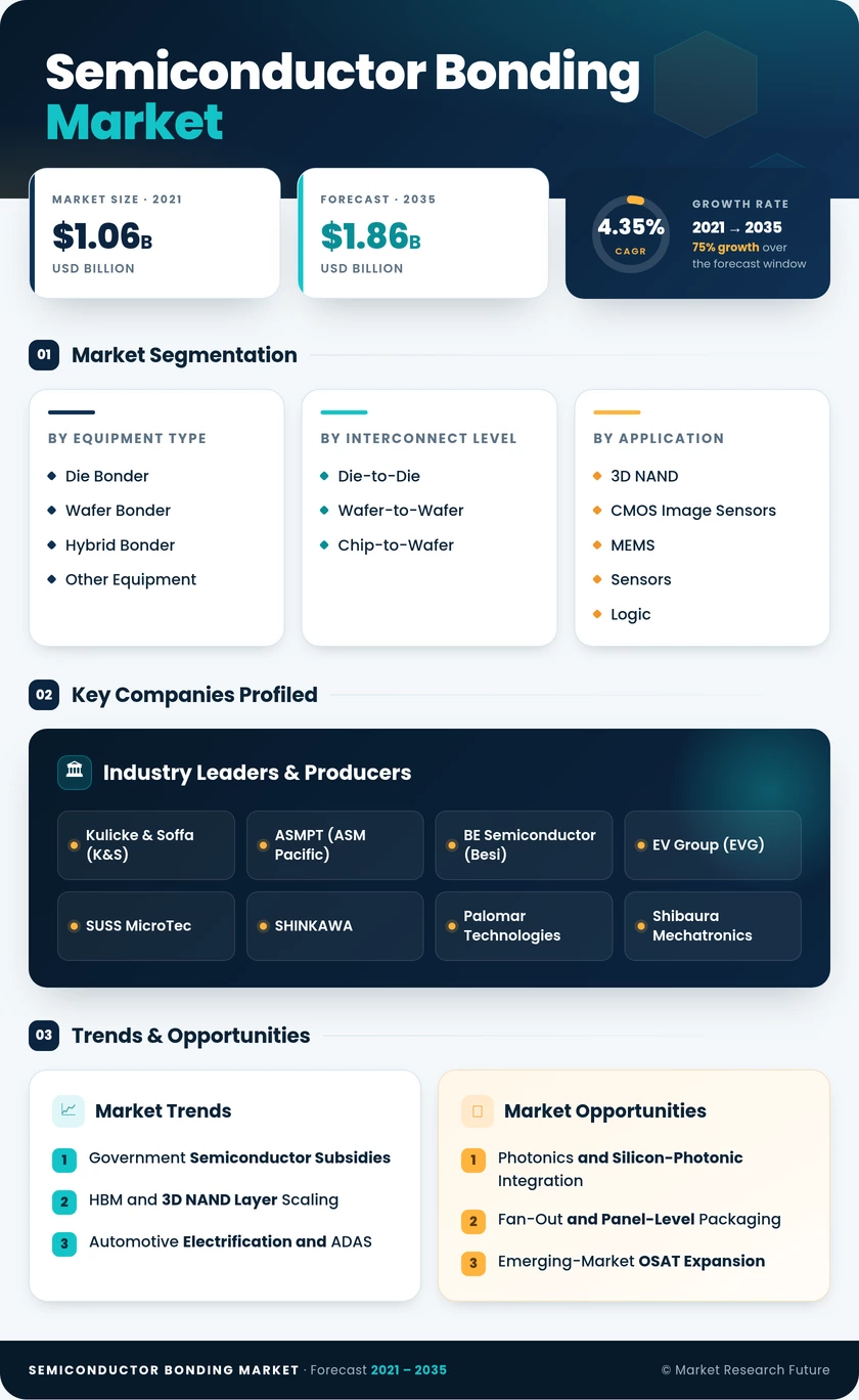
CAGR (2026-2035)4.35%
2021 Market Size1.21 USD Billion
2025 Market Size1.27 USD Billion
Key Players
Kulicke & Soffa
ASMPT
BE Semiconductor
EV Group
SUSS MicroTec
SHINKAWA
Opportunities
  • Photonics and Silicon-Photonic Integration
  • Fan-Out and Panel-Level Packaging
  • Emerging-Market OSAT Expansion
  1. 1 Market Overview |
    1. 1.1 Study Assumptions & Market Definition |
    2. 1.2 Scope of the Study |
    3. 1.3 Research Methodology
  2. 2 Market Summary & Key Takeaways
  3. 3 Market Dynamics |
    1. 3.1 Market Drivers Analysis | |
      1. 3.1.1 Government Semiconductor Subsidies | |
      2. 3.1.2 HBM and 3D NAND Layer Scaling | |
      3. 3.1.3 Automotive Electrification and ADAS | |
      4. 3.1.4 Chiplet Standardization (UCIe, BoW) | |
      5. 3.1.5 CMOS Image Sensor Stacking | |
      6. 3.1.6 Advanced Display and AR/VR Silicon | |
      7. 3.1.7 Edge AI and IoT Module Packaging |
    2. 3.2 Market Restraints Analysis | |
      1. 3.2.1 Alignment Precision and Yield Loss | |
      2. 3.2.2 High Capital Intensity of Hybrid Bonders | |
      3. 3.2.3 Export Controls and Geopolitical Risk | |
      4. 3.2.4 Shortage of Process Engineers | |
      5. 3.2.5 Thermal Management in Dense Stacks |
    3. 3.3 Market Opportunity Analysis | |
      1. 3.3.1 Photonics and Silicon-Photonic Integration | |
      2. 3.3.2 Fan-Out and Panel-Level Packaging | |
      3. 3.3.3 Emerging-Market OSAT Expansion | |
      4. 3.3.4 Equipment-as-a-Service and Data Monetization | |
      5. 3.3.5 Biomedical MEMS and Wearable Sensors |
    4. 3.4 Industry Value Chain Analysis |
    5. 3.5 Porter's Five Forces Analysis
  4. 4 Global Semiconductor Bonding Market Size & Forecast (2021–2035) |
    1. 4.1 Historical Market Size (2021–2025) |
    2. 4.2 Current & Forecast Market Size (2026–2035) |
    3. 4.3 Market Size by Revenue (USD billion) |
    4. 4.4 Year-over-Year Growth Analysis
  5. 5 Segmentation Analysis |
    1. 5.1 By Equipment Type | |
      1. 5.1.1 Die Bonder | |
      2. 5.1.2 Wafer Bonder | |
      3. 5.1.3 Hybrid Bonder | |
      4. 5.1.4 Other Equipment |
    2. 5.2 By Interconnect Level | |
      1. 5.2.1 Die-to-Die | |
      2. 5.2.2 Wafer-to-Wafer | |
      3. 5.2.3 Chip-to-Wafer |
    3. 5.3 By Application | |
      1. 5.3.1 3D NAND | |
      2. 5.3.2 CMOS Image Sensors | |
      3. 5.3.3 MEMS and Sensors | |
      4. 5.3.4 Logic and HPC | |
      5. 5.3.5 RF and Communication | |
      6. 5.3.6 Other Applications |
    4. 5.4 By End-Use Industry | |
      1. 5.4.1 Consumer Electronics | |
      2. 5.4.2 Automotive and Mobility | |
      3. 5.4.3 Data Center and Cloud | |
      4. 5.4.4 Telecom and Infrastructure | |
      5. 5.4.5 Industrial and Medical
  6. 6 Regional Analysis |
    1. 6.1 North America | |
      1. 6.1.1 United States | |
      2. 6.1.2 Canada | |
      3. 6.1.3 Mexico |
    2. 6.2 Europe | |
      1. 6.2.1 Germany | |
      2. 6.2.2 United Kingdom | |
      3. 6.2.3 France | |
      4. 6.2.4 Italy | |
      5. 6.2.5 Spain | |
      6. 6.2.6 Nordic Countries | |
      7. 6.2.7 Russia | |
      8. 6.2.8 Rest of Europe |
    3. 6.3 Asia-Pacific | |
      1. 6.3.1 China | |
      2. 6.3.2 Japan | |
      3. 6.3.3 South Korea | |
      4. 6.3.4 India | |
      5. 6.3.5 ASEAN | |
      6. 6.3.6 Rest of Asia-Pacific |
    4. 6.4 South America | |
      1. 6.4.1 Brazil | |
      2. 6.4.2 Argentina | |
      3. 6.4.3 Rest of South America |
    5. 6.5 Middle East & Africa | |
      1. 6.5.1 Saudi Arabia | |
      2. 6.5.2 UAE | |
      3. 6.5.3 South Africa | |
      4. 6.5.4 Egypt | |
      5. 6.5.5 Rest of MEA
  7. 7 Competitive Landscape |
    1. 7.1 Market Share Analysis (2025) |
    2. 7.2 Competitive Benchmarking Matrix |
    3. 7.3 Company Profiles | |
      1. 7.3.1 Kulicke & Soffa (K&S) | |
      2. 7.3.2 ASMPT (ASM Pacific Technology) | |
      3. 7.3.3 BE Semiconductor Industries (Besi) | |
      4. 7.3.4 EV Group (EVG) | |
      5. 7.3.5 SUSS MicroTec | |
      6. 7.3.6 SHINKAWA | |
      7. 7.3.7 Palomar Technologies | |
      8. 7.3.8 Shibaura Mechatronics | |
      9. 7.3.9 Toray Engineering | |
      10. 7.3.10 Fasford Technology
  8. 8 Future Outlook & Strategic Recommendations (2026–2035) |
    1. 8.1 AI-Driven Process Optimization |
    2. 8.2 Chiplet Economy and Heterogeneous Integration |
    3. 8.3 Sustainability and Green Packaging |
    4. 8.4 Geopolitical Supply-Chain Reconfiguration
  9. 9 Recent Developments & News
  10. 10 Frequently Asked Questions (FAQs)
  11. 11 Report Scope & Methodology |
    1. 11.1 Study Period & Base Year |
    2. 11.2 Data Sources & Citations |
    3. 11.3 Abbreviations
  12. 12 LIST OF TABLES |
  13. TABLE 1 Global Semiconductor Bonding Market Size & Forecast, by Revenue (USD billion), 2021–2035 |
  14. TABLE 2 Global Semiconductor Bonding Market – Year-over-Year Growth Analysis, 2021–2035 |
  15. TABLE 3 Global Semiconductor Bonding Market – Driver Impact Analysis |
  16. TABLE 4 Global Semiconductor Bonding Market – Restraint Impact Analysis |
  17. TABLE 5 Global Semiconductor Bonding Market Size, by Equipment Type, 2021–2035 (USD billion) |
  18. TABLE 6 Global Semiconductor Bonding Market Size, by Interconnect Level, 2021–2035 (USD billion) |
  19. TABLE 7 Global Semiconductor Bonding Market Size, by Application, 2021–2035 (USD billion) |
  20. TABLE 8 Global Semiconductor Bonding Market Size, by End-Use Industry, 2021–2035 (USD billion) |
  21. TABLE 9 Global Semiconductor Bonding Market Size, by Region, 2021–2035 (USD billion) |
  22. TABLE 10 North America Semiconductor Bonding Market Size, by Country, 2021–2035 (USD billion) |
  23. TABLE 11 Europe Semiconductor Bonding Market Size, by Country, 2021–2035 (USD billion) |
  24. TABLE 12 Asia-Pacific Semiconductor Bonding Market Size, by Country, 2021–2035 (USD billion) |
  25. TABLE 13 South America Semiconductor Bonding Market Size, by Country, 2021–2035 (USD billion) |
  26. TABLE 14 Middle East & Africa Semiconductor Bonding Market Size, by Country, 2021–2035 (USD billion) |
  27. TABLE 15 Competitive Benchmarking Matrix – Global Semiconductor Bonding Market, 2025 |
  28. TABLE 16 Company Profiles – Key Players, Global Semiconductor Bonding Market |
  29. TABLE 17 Recent Developments & Strategic Announcements, 2024–2025 |
  30. TABLE 18 North America Semiconductor Bonding Market Size, by Equipment Type, 2021–2035 (USD billion) |
  31. TABLE 19 North America Semiconductor Bonding Market Size, by Interconnect Level, 2021–2035 (USD billion) |
  32. TABLE 20 North America Semiconductor Bonding Market Size, by Application, 2021–2035 (USD billion) |
  33. TABLE 21 North America Semiconductor Bonding Market Size, by End-Use Industry, 2021–2035 (USD billion) |
  34. TABLE 22 Europe Semiconductor Bonding Market Size, by Equipment Type, 2021–2035 (USD billion) |
  35. TABLE 23 Europe Semiconductor Bonding Market Size, by Interconnect Level, 2021–2035 (USD billion) |
  36. TABLE 24 Europe Semiconductor Bonding Market Size, by Application, 2021–2035 (USD billion) |
  37. TABLE 25 Europe Semiconductor Bonding Market Size, by End-Use Industry, 2021–2035 (USD billion) |
  38. TABLE 26 Asia-Pacific Semiconductor Bonding Market Size, by Equipment Type, 2021–2035 (USD billion) |
  39. TABLE 27 Asia-Pacific Semiconductor Bonding Market Size, by Interconnect Level, 2021–2035 (USD billion) |
  40. TABLE 28 Asia-Pacific Semiconductor Bonding Market Size, by Application, 2021–2035 (USD billion) |
  41. TABLE 29 Asia-Pacific Semiconductor Bonding Market Size, by End-Use Industry, 2021–2035 (USD billion) |
  42. TABLE 30 South America Semiconductor Bonding Market Size, by Equipment Type, 2021–2035 (USD billion) |
  43. TABLE 31 South America Semiconductor Bonding Market Size, by Interconnect Level, 2021–2035 (USD billion) |
  44. TABLE 32 South America Semiconductor Bonding Market Size, by Application, 2021–2035 (USD billion) |
  45. TABLE 33 South America Semiconductor Bonding Market Size, by End-Use Industry, 2021–2035 (USD billion) |
  46. TABLE 34 Middle East & Africa Semiconductor Bonding Market Size, by Equipment Type, 2021–2035 (USD billion) |
  47. TABLE 35 Middle East & Africa Semiconductor Bonding Market Size, by Interconnect Level, 2021–2035 (USD billion) |
  48. TABLE 36 Middle East & Africa Semiconductor Bonding Market Size, by Application, 2021–2035 (USD billion) |
  49. TABLE 37 Middle East & Africa Semiconductor Bonding Market Size, by End-Use Industry, 2021–2035 (USD billion) |
  50. TABLE 38 United States Semiconductor Bonding Market Size, by Equipment Type, 2021–2035 (USD billion) |
  51. TABLE 39 United States Semiconductor Bonding Market Size, by Interconnect Level, 2021–2035 (USD billion) |
  52. TABLE 40 United States Semiconductor Bonding Market Size, by Application, 2021–2035 (USD billion) |
  53. TABLE 41 United States Semiconductor Bonding Market Size, by End-Use Industry, 2021–2035 (USD billion) |
  54. TABLE 42 Canada Semiconductor Bonding Market Size, by Equipment Type, 2021–2035 (USD billion) |
  55. TABLE 43 Canada Semiconductor Bonding Market Size, by Interconnect Level, 2021–2035 (USD billion) |
  56. TABLE 44 Canada Semiconductor Bonding Market Size, by Application, 2021–2035 (USD billion) |
  57. TABLE 45 Canada Semiconductor Bonding Market Size, by End-Use Industry, 2021–2035 (USD billion) |
  58. TABLE 46 Mexico Semiconductor Bonding Market Size, by Equipment Type, 2021–2035 (USD billion) |
  59. TABLE 47 Mexico Semiconductor Bonding Market Size, by Interconnect Level, 2021–2035 (USD billion) |
  60. TABLE 48 Mexico Semiconductor Bonding Market Size, by Application, 2021–2035 (USD billion) |
  61. TABLE 49 Mexico Semiconductor Bonding Market Size, by End-Use Industry, 2021–2035 (USD billion) |
  62. TABLE 50 Germany Semiconductor Bonding Market Size, by Equipment Type, 2021–2035 (USD billion) |
  63. TABLE 51 Germany Semiconductor Bonding Market Size, by Interconnect Level, 2021–2035 (USD billion) |
  64. TABLE 52 Germany Semiconductor Bonding Market Size, by Application, 2021–2035 (USD billion) |
  65. TABLE 53 Germany Semiconductor Bonding Market Size, by End-Use Industry, 2021–2035 (USD billion) |
  66. TABLE 54 United Kingdom Semiconductor Bonding Market Size, by Equipment Type, 2021–2035 (USD billion) |
  67. TABLE 55 United Kingdom Semiconductor Bonding Market Size, by Interconnect Level, 2021–2035 (USD billion) |
  68. TABLE 56 United Kingdom Semiconductor Bonding Market Size, by Application, 2021–2035 (USD billion) |
  69. TABLE 57 United Kingdom Semiconductor Bonding Market Size, by End-Use Industry, 2021–2035 (USD billion) |
  70. TABLE 58 France Semiconductor Bonding Market Size, by Equipment Type, 2021–2035 (USD billion) |
  71. TABLE 59 France Semiconductor Bonding Market Size, by Interconnect Level, 2021–2035 (USD billion) |
  72. TABLE 60 France Semiconductor Bonding Market Size, by Application, 2021–2035 (USD billion) |
  73. TABLE 61 France Semiconductor Bonding Market Size, by End-Use Industry, 2021–2035 (USD billion) |
  74. TABLE 62 China Semiconductor Bonding Market Size, by Equipment Type, 2021–2035 (USD billion) |
  75. TABLE 63 China Semiconductor Bonding Market Size, by Interconnect Level, 2021–2035 (USD billion) |
  76. TABLE 64 China Semiconductor Bonding Market Size, by Application, 2021–2035 (USD billion) |
  77. TABLE 65 China Semiconductor Bonding Market Size, by End-Use Industry, 2021–2035 (USD billion) |
  78. TABLE 66 Japan Semiconductor Bonding Market Size, by Equipment Type, 2021–2035 (USD billion) |
  79. TABLE 67 Japan Semiconductor Bonding Market Size, by Interconnect Level, 2021–2035 (USD billion) |
  80. TABLE 68 Japan Semiconductor Bonding Market Size, by Application, 2021–2035 (USD billion) |
  81. TABLE 69 Japan Semiconductor Bonding Market Size, by End-Use Industry, 2021–2035 (USD billion) |
  82. TABLE 70 South Korea Semiconductor Bonding Market Size, by Equipment Type, 2021–2035 (USD billion) |
  83. TABLE 71 South Korea Semiconductor Bonding Market Size, by Interconnect Level, 2021–2035 (USD billion) |
  84. TABLE 72 South Korea Semiconductor Bonding Market Size, by Application, 2021–2035 (USD billion) |
  85. TABLE 73 South Korea Semiconductor Bonding Market Size, by End-Use Industry, 2021–2035 (USD billion) |
  86. TABLE 74 India Semiconductor Bonding Market Size, by Equipment Type, 2021–2035 (USD billion) |
  87. TABLE 75 India Semiconductor Bonding Market Size, by Interconnect Level, 2021–2035 (USD billion) |
  88. TABLE 76 India Semiconductor Bonding Market Size, by Application, 2021–2035 (USD billion) |
  89. TABLE 77 India Semiconductor Bonding Market Size, by End-Use Industry, 2021–2035 (USD billion) |
  90. TABLE 78 Brazil Semiconductor Bonding Market Size, by Equipment Type, 2021–2035 (USD billion) |
  91. TABLE 79 Brazil Semiconductor Bonding Market Size, by Interconnect Level, 2021–2035 (USD billion) |
  92. TABLE 80 Brazil Semiconductor Bonding Market Size, by Application, 2021–2035 (USD billion) |
  93. TABLE 81 Brazil Semiconductor Bonding Market Size, by End-Use Industry, 2021–2035 (USD billion) |
  94. TABLE 82 Saudi Arabia Semiconductor Bonding Market Size, by Equipment Type, 2021–2035 (USD billion) |
  95. TABLE 83 Saudi Arabia Semiconductor Bonding Market Size, by Interconnect Level, 2021–2035 (USD billion) |
  96. TABLE 84 Saudi Arabia Semiconductor Bonding Market Size, by Application, 2021–2035 (USD billion) |
  97. TABLE 85 Saudi Arabia Semiconductor Bonding Market Size, by End-Use Industry, 2021–2035 (USD billion) |
  98. TABLE 86 UAE Semiconductor Bonding Market Size, by Equipment Type, 2021–2035 (USD billion) |
  99. TABLE 87 UAE Semiconductor Bonding Market Size, by Interconnect Level, 2021–2035 (USD billion) |
  100. TABLE 88 UAE Semiconductor Bonding Market Size, by Application, 2021–2035 (USD billion) |
  101. TABLE 89 UAE Semiconductor Bonding Market Size, by End-Use Industry, 2021–2035 (USD billion) |
  102. TABLE 90 Report Scope & Methodology Summary
  103. 13 LIST OF FIGURES |
  104. FIGURE 1 Semiconductor Bonding Market Dynamics Overview |
  105. FIGURE 2 Value Chain Analysis – Semiconductor Bonding Market |
  106. FIGURE 3 Porter's Five Forces Analysis – Semiconductor Bonding Market |
  107. FIGURE 4 Global Semiconductor Bonding Market Size Trend & Forecast (USD billion), 2021–2035 |
  108. FIGURE 5 Semiconductor Bonding Market Share, by Equipment Type (%), 2025 |
  109. FIGURE 6 Semiconductor Bonding Market Share, by Interconnect Level (%), 2025 |
  110. FIGURE 7 Semiconductor Bonding Market Share, by Application (%), 2025 |
  111. FIGURE 8 Semiconductor Bonding Market Share, by End-Use Industry (%), 2025 |
  112. FIGURE 9 Semiconductor Bonding Market Share, by Region (%), 2025 |
  113. FIGURE 10 North America Semiconductor Bonding Market Size Trend, 2021–2035 |
  114. FIGURE 11 Europe Semiconductor Bonding Market Size Trend, 2021–2035 |
  115. FIGURE 12 Asia-Pacific Semiconductor Bonding Market Size Trend, 2021–2035 |
  116. FIGURE 13 South America Semiconductor Bonding Market Size Trend, 2021–2035 |
  117. FIGURE 14 Middle East & Africa Semiconductor Bonding Market Size Trend, 2021–2035 |
  118. FIGURE 15 Competitive Landscape Heat Map – Semiconductor Bonding Market, 2025

Segmentation Quick Reference

DimensionSub-SegmentsDominant SegmentFastest Growing Segment
Equipment TypeDie Bonder, Wafer Bonder, Hybrid Bonder, Other EquipmentDie Bonder (39.5% share, 2025)Hybrid Bonder (4.60% CAGR)
Interconnect LevelDie-to-Die, Wafer-to-Wafer, Chip-to-WaferDie-to-Die (57.5% share, 2025)Wafer-to-Wafer (4.85% CAGR)
Application3D NAND, CMOS Image Sensors, MEMS and Sensors, Logic and HPC, RF and Communication, Other Applications3D NAND (23.7% share, 2025)CMOS Image Sensors (5.0% CAGR)
End-Use IndustryConsumer Electronics, Automotive and Mobility, Data Center and Cloud, Telecom and Infrastructure, Industrial and MedicalConsumer Electronics (41.0% share, 2025)Automotive and Mobility (5.40% CAGR)
GeographyAsia-Pacific, North America, Europe, South America, the Middle East & AfricaAsia-Pacific (44.5% share, 2025)Asia-Pacific (5.28% CAGR)


Market Segmentation Overview

By Equipment Type

Sub-SegmentKey Trend
Die BonderDominant platform for high-volume memory and consumer IC assembly; incremental throughput gains via AI-guided placement
Wafer BonderEssential for MEMS sealing, CIS fabrication, and power device manufacturing
Hybrid BonderFastest-growing category driven by HBM, logic-on-logic stacking, and chiplet integration
Other EquipmentIncludes specialty R&D tools and emerging panel-level bonding systems


Die bonder equipment remains the most widely installed bonding tool category, serving the broadest range of applications from consumer IC assembly to automotive power modules. Hybrid bonders are commanding the highest investment growth as foundries and IDMs transition to copper-to-copper direct bonding for next-generation 3D architectures.

By Interconnect Level

Sub-SegmentKey Trend
Die-to-DieLargest segment: enables mixing dies from different process nodes for disaggregated designs.
Wafer-to-WaferHighest throughput for uniform devices; growth led by CIS and MEMS applications
Chip-to-WaferEmerging approach for HBM stacking and known-good-die integration


Die-to-die bonding underpins the chiplet revolution by enabling designers to combine compute, memory, and I/O tiles from separate fabs. Wafer-to-wafer bonding offers superior alignment precision for devices that use identical dies on both wafer halves, making it the preferred approach for backside-illuminated image sensors.

By Application

Sub-SegmentKey Trend
3D NANDLayer counts exceeding 200 drive repeated bonding and thinning cycles per device.
CMOS Image SensorsMulti-camera smartphones and automotive vision expand wafer-bonded CIS demand.
MEMS and SensorsHermetic sealing and low-temperature bonding support medical and industrial IoT sensors
Logic and HPCAI accelerators and data-center processors adopt hybrid bonding for performance.
RF and Communication5G front-end module assembly requires precision die-attach processes
Other ApplicationsIncludes LED, power devices, and photonic packaging


3D NAND applications consume the largest share of bonding equipment capacity globally, as each incremental generation of vertical flash memory adds bonding process steps. CMOS image sensors represent the fastest-growing application category, propelled by the adoption of multi-camera arrays and the integration of LiDAR sensors in vehicles.

By End-Use Industry

Sub-SegmentKey Trend
Consumer ElectronicsLargest end-use, driven by smartphone, wearable, and gaming device volumes
Automotive and MobilityFastest-growing; EV power modules and ADAS sensors expand semiconductor content per vehicle
Data Center and CloudAI training and inference chip packaging intensify bonding demand.
Telecom and Infrastructure5G base station rollout sustains bonding tool orders for RF modules
Industrial and MedicalPrecision sensors and biomedical MEMS require specialized bonding processes.


Consumer electronics continue to dominate end-use demand due to the massive unit volumes associated with smartphone and wearable device production. Automotive and mobility is the fastest-growing vertical, as vehicle electrification and advanced driver-assistance systems multiply the bonded semiconductor content in each automobile.

By Geography

Sub-SegmentKey Trend
Asia-PacificLargest and fastest-growing concentrated OSAT and memory fab capacity
North AmericaSecond-largest; CHIPS Act packaging investments drive expansion
EuropeAutomotive power module bonding; EU Chips Act funding
South AmericaEmerging: Manaus electronics zone and telecom assembly
Middle East & AfricaNascent; defense electronics and Vision 2030 industrialization


Asia-Pacific commands the largest share of the global market owing to its dense ecosystem of OSATs, foundries, and memory manufacturers in Taiwan, South Korea, China, and Japan. North America is the second-largest region, bolstered by federal subsidies targeting domestic advanced-packaging capacity and growing AI chip assembly demand.


Download PDF ×

We do not share your information with anyone. However, we may send you emails based on your report interest from time to time. You may contact us at any time to opt-out.