×
Request Free Sample ×

Kindly complete the form below to receive a free sample of this Report

* Please use a valid business email

Leading companies partner with us for data-driven Insights

clients tt-cursor
Hero Background

US GaAs Wafer Market

ID: MRFR/SEM/16280-HCR
200 Pages
Garvit Vyas
October 2025

US GaAs Wafer Market Research Report By Production Method (Vertical Gradient Freeze, Liquid Encapsulated Czochralski, Molecular Beam Epitaxy, Metal Organic Vapor Phase Epitaxy) and By Applications (Mobile Device, Photovoltaic Devices, Wireless Communication, Optoelectronic Device, Aerospace & Defense, Others) - Forecast to 2035

Share:
Download PDF ×

We do not share your information with anyone. However, we may send you emails based on your report interest from time to time. You may contact us at any time to opt-out.

US GaAs Wafer Market Infographic
Purchase Options

US GaAs Wafer Market Summary

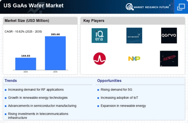
As per MRFR analysis, the US GaAs wafer market size was estimated at 130.2 USD Million in 2024. The US gaas wafer market is projected to grow from 144.03 USD Million in 2025 to 395.0 USD Million by 2035, exhibiting a compound annual growth rate (CAGR) of 10.62% during the forecast period 2025 - 2035.

Key Market Trends & Highlights

The US GaAs wafer market is experiencing robust growth driven by technological advancements and increasing demand across various sectors.

  • Technological advancements are propelling the US GaAs wafer market towards enhanced performance and efficiency.
  • The telecommunications segment remains the largest, driven by the rising demand for 5G infrastructure and IoT devices.
  • Energy efficiency is becoming a focal point, influencing the design and application of GaAs wafers in consumer electronics.
  • Key market drivers include the surge in consumer electronics and the expansion of 5G infrastructure, which are significantly shaping market dynamics.

Market Size & Forecast

2024 Market Size 130.2 (USD Million)
2035 Market Size 395.0 (USD Million)
CAGR (2025 - 2035) 10.62%

Major Players

IQE (GB), Skyworks Solutions (US), Qorvo (US), Broadcom (US), NXP Semiconductors (NL), Aixtron (DE), Sumitomo Electric (JP), Mitsubishi Electric (JP), OSRAM (DE)

US GaAs Wafer Market Trends

The GaAs wafer market is currently experiencing notable growth, driven by advancements in technology and increasing demand for high-performance electronic devices. The shift towards more efficient and compact components in sectors such as telecommunications, consumer electronics, and automotive applications appears to be a significant factor influencing this trend. As industries continue to innovate, the need for gallium arsenide wafers, known for their superior electronic properties, is likely to expand. This growth trajectory suggests a robust future for the market, with potential opportunities for manufacturers and suppliers to enhance their production capabilities and meet evolving consumer needs. In addition, the ongoing research and development efforts in the semiconductor sector indicate a strong commitment to improving the performance and efficiency of gaas wafers. The integration of these materials into next-generation technologies, such as 5G and beyond, may further bolster market demand. Furthermore, the increasing focus on sustainability and energy efficiency in manufacturing processes could lead to new methodologies that enhance the production of gaas wafers. Overall, the GaAs wafer market seems poised for continued expansion, driven by technological advancements and a growing emphasis on high-performance applications.

Technological Advancements

Recent innovations in semiconductor technology are significantly impacting the gaas wafer market. Enhanced fabrication techniques and improved material quality are enabling the production of wafers with superior performance characteristics. This trend is likely to attract more investments and research initiatives aimed at further enhancing the capabilities of gaas wafers.

Rising Demand in Telecommunications

The increasing deployment of advanced communication networks, particularly in the telecommunications sector, is driving the demand for gaas wafers. As the industry transitions to higher frequency applications, the unique properties of gallium arsenide are becoming increasingly valuable, suggesting a sustained growth trajectory in this area.

Focus on Energy Efficiency

There is a growing emphasis on energy-efficient solutions across various industries, which is influencing the gaas wafer market. Manufacturers are exploring ways to optimize production processes and reduce energy consumption, potentially leading to more sustainable practices and products in the future.

US GaAs Wafer Market Drivers

Surge in Consumer Electronics

The GaAs wafer market is experiencing a notable surge in demand driven by the increasing production of consumer electronics. As devices such as smartphones, tablets, and laptops become more prevalent, the need for high-performance components is paramount. GaAs wafers, known for their superior efficiency and performance in high-frequency applications, are becoming essential in the manufacturing of these devices. In 2025, the consumer electronics sector is projected to contribute approximately $200 billion to the overall semiconductor market, with GaAs wafers playing a critical role in this growth. This trend indicates a robust future for the gaas wafer market, as manufacturers seek to enhance device capabilities while maintaining compact sizes and energy efficiency.

Expansion of 5G Infrastructure

The ongoing expansion of 5G infrastructure in the US is significantly impacting the gaas wafer market. As telecommunications companies invest heavily in upgrading their networks, the demand for high-frequency components is surging. GaAs wafers are particularly suited for 5G applications due to their ability to operate at higher frequencies with lower power consumption. It is estimated that the 5G market will reach $300 billion by 2025, with GaAs technology being a key enabler of this transition. This growth presents a substantial opportunity for the gaas wafer market, as it aligns with the increasing need for faster and more reliable communication technologies.

Advancements in Aerospace and Defense

The aerospace and defense sectors are increasingly adopting GaAs technology, which is driving growth in the gaas wafer market. GaAs wafers are utilized in various applications, including satellite communications, radar systems, and electronic warfare. The US government is projected to allocate over $700 billion to defense spending in 2025, with a significant portion directed towards advanced technologies that enhance operational capabilities. This investment is likely to bolster the demand for GaAs wafers, as they provide the necessary performance and reliability required in critical defense applications. The GaAs wafer market is thus positioned to benefit from this upward trend in defense-related expenditures.

Growth in Renewable Energy Technologies

The shift towards renewable energy technologies is influencing the gaas wafer market positively. GaAs wafers are increasingly being used in solar cells and other renewable energy applications due to their high efficiency and performance. The US solar market is expected to grow to $30 billion by 2025, with GaAs technology playing a pivotal role in enhancing energy conversion efficiencies. This trend suggests that the GaAs wafer market could see a substantial increase in demand as manufacturers seek to develop more efficient solar panels and energy systems. The integration of GaAs technology in renewable energy solutions indicates a promising future for the market.

Emergence of Internet of Things (IoT) Devices

The rise of Internet of Things (IoT) devices is creating new opportunities for the gaas wafer market. As more devices become interconnected, the demand for efficient and high-performance components is escalating. GaAs wafers are particularly advantageous in IoT applications due to their ability to support high-frequency operations while minimizing power consumption. The IoT market in the US is projected to reach $1 trillion by 2025, with GaAs technology likely to play a crucial role in the development of smart devices and systems. This growth in IoT applications suggests a favorable outlook for the gaas wafer market, as manufacturers adapt to meet the evolving needs of this expanding sector.

Market Segment Insights

By Production Method: Vertical Gradient Freeze (Largest) vs. Metal-Organic Vapor Phase Epitaxy (Fastest-Growing)

In the US gaas wafer market, the production method segment is prominently led by the Vertical Gradient Freeze (VGF), capturing a significant share due to its efficient crystal growth and superior quality output. Following closely are Liquid Encapsulated Czochralski (LEC) and Molecular Beam Epitaxy (MBE), which also hold notable positions although they are not as dominant. The Metal-Organic Vapor Phase Epitaxy (MOVPE) method, while smaller in market share, is rapidly gaining traction as its applications in advanced optoelectronic devices expand. Current growth trends in the production method segment are influenced by the increasing demand for high-efficiency devices in the electronics and telecommunication sectors. The emphasis on renewable energy solutions is further propelling the need for high-quality wafers produced using methods like MOVPE. With enhanced capabilities to produce complex structures, these methods are becoming integral to technological advancements in semiconductor applications, contributing to a robust growth outlook for the coming years.

Vertical Gradient Freeze (Dominant) vs. Metal-Organic Vapor Phase Epitaxy (Emerging)

Vertical Gradient Freeze (VGF) is recognized as the dominant production method in the market, mainly due to its ability to produce large diameter wafers with outstanding uniformity and low defect densities. This method supports the manufacturing of high-performance devices, making it a preferred choice among industry players. In contrast, Metal-Organic Vapor Phase Epitaxy (MOVPE) is emerging rapidly due to its adaptability in producing complex multilayer structures essential for modern applications in optoelectronics. MOVPE’s flexibility in material choice and its capability to support advanced compound semiconductor manufacturing are driving its growth, positioning it as a key player in the evolving landscape of the US gaas wafer market.

By Applications: Mobile Devices (Largest) vs. Wireless Communication (Fastest-Growing)

In the US gaas wafer market, the Applications segment is predominantly led by Mobile Devices, which holds a significant market share due to the increasing demand for advanced smartphones and tablets. This segment capitalizes on the need for efficient power consumption and enhanced performance, which are critical in today's technology-driven landscape. Following closely, Wireless Communication is also experiencing growth, driven by the expansion of 5G technology and related applications, leading to a dynamic shift in market dynamics. Growth trends indicate that while Mobile Devices continue to dominate the share, Wireless Communication is emerging as the fastest-growing segment as businesses and consumers alike invest in next-generation communication capabilities. The transition towards more robust and flexible wireless networks is driving innovation and fuelling demand for GaAs wafers specifically designed for these applications. The rise of IoT and smart devices further accelerates this trend, paving the way for enhanced product development and market opportunities.

Mobile Devices (Dominant) vs. Photovoltaic Devices (Emerging)

Mobile Devices represent the dominant application within the US gaas wafer market, primarily due to their critical role in smartphones and tablets that demand high efficiency and performance. As technology evolves, these devices require GaAs wafers capable of supporting faster processing speeds and improved battery life, making them essential for manufacturers aiming to stay competitive. On the other hand, Photovoltaic Devices, which are emerging within this segment, are gaining traction as renewable energy becomes a priority in sustainability efforts. This segment benefits from technological advancements that enhance the efficiency of solar cells, motivating manufacturers to invest in GaAs technology for improved performance and cost-efficiency. The growing trend toward green technologies positions Photovoltaic Devices as a key player in the evolving market landscape.

Get more detailed insights about US GaAs Wafer Market

Key Players and Competitive Insights

The GaAs wafer market is currently characterized by a dynamic competitive landscape, driven by advancements in technology and increasing demand for high-performance electronic devices. Key players such as Skyworks Solutions (US), Qorvo (US), and Broadcom (US) are at the forefront, each adopting distinct strategies to enhance their market positioning. Skyworks Solutions (US) focuses on innovation in RF solutions, while Qorvo (US) emphasizes strategic partnerships to expand its product offerings. Broadcom (US), on the other hand, is leveraging its extensive portfolio to cater to diverse applications, thereby shaping a competitive environment that is both collaborative and competitive.

In terms of business tactics, companies are increasingly localizing manufacturing to mitigate supply chain disruptions and optimize operational efficiency. The market structure appears moderately fragmented, with several players vying for market share. However, the collective influence of major companies like Skyworks Solutions (US) and Qorvo (US) suggests a trend towards consolidation, as these firms seek to enhance their competitive edge through strategic collaborations and technological advancements.

In October 2025, Skyworks Solutions (US) announced a partnership with a leading automotive manufacturer to develop advanced GaAs-based components for electric vehicles. This strategic move is likely to position Skyworks at the forefront of the burgeoning electric vehicle market, aligning with the industry's shift towards high-efficiency power management solutions. The collaboration underscores the importance of innovation in meeting the evolving demands of the automotive sector.

In September 2025, Qorvo (US) unveiled a new line of GaAs wafers designed specifically for 5G applications, enhancing its product portfolio in a rapidly growing segment. This launch not only reinforces Qorvo's commitment to technological advancement but also indicates a strategic focus on capturing market share in the 5G infrastructure space, which is expected to witness substantial growth in the coming years.

In August 2025, Broadcom (US) completed the acquisition of a semiconductor company specializing in GaAs technology, further expanding its capabilities in the high-frequency market. This acquisition is significant as it allows Broadcom to integrate advanced GaAs solutions into its existing product lines, thereby enhancing its competitive positioning and enabling it to offer more comprehensive solutions to its customers.

As of November 2025, current competitive trends in the GaAs wafer market include a strong emphasis on digitalization, sustainability, and the integration of AI technologies. Strategic alliances are increasingly shaping the landscape, as companies recognize the need for collaboration to drive innovation and meet market demands. Looking ahead, competitive differentiation is likely to evolve from traditional price-based competition to a focus on technological innovation, supply chain reliability, and sustainable practices, reflecting the industry's response to changing consumer preferences and regulatory pressures.

Key Companies in the US GaAs Wafer Market market include

Industry Developments

The US GaAs Wafer Market is currently experiencing significant dynamics, particularly with ongoing technological advancements and shifts in consumer demand. Companies like Transphorm, Skyworks Solutions, and Wolfspeed are actively developing innovative applications to integrate gallium arsenide semiconductors in various electronic devices, boosting market interest. Recently, in August 2023, Qorvo announced an expansion of its manufacturing capabilities in the US to meet increasing demand for 5G and RF solutions, indicating a trend towards local sourcing and production.

Additionally, Texas Instruments and Intel have ramped up their investments in Research and Development for GaAs technologies, further demonstrating the high growth potential in this sector. In terms of mergers and acquisitions, Broadcom's acquisition of an RF component manufacturer in July 2023 marked a notable move, which aims to enhance its portfolio in semiconductor solutions. Overall, the valuation of companies within the US GaAs Wafer Market is on an upward trajectory as they leverage advanced materials and enhanced fabrication techniques to meet the growing demand in telecommunications, automotive, and consumer electronics.

Investments and strategic partnerships are expected to shape the landscape, providing strong signals of growth in the market.

Future Outlook

US GaAs Wafer Market Future Outlook

The GaAs wafer market is projected to grow at a 10.62% CAGR from 2024 to 2035, driven by advancements in semiconductor technology and increasing demand for high-frequency applications.

New opportunities lie in:

  • Development of specialized GaAs wafers for 5G telecommunications equipment.
  • Expansion into renewable energy sectors with GaAs solar cells.
  • Investment in R&D for next-generation GaAs materials and manufacturing processes.

By 2035, the GaAs wafer market is expected to achieve substantial growth and innovation.

Market Segmentation

US GaAs Wafer Market Applications Outlook

  • Mobile Devices
  • Photovoltaic Devices
  • Wireless Communication
  • Optoelectronic Device
  • Aerospace & Defense
  • Others

US GaAs Wafer Market Production Method Outlook

  • Vertical Gradient Freeze (VGF)
  • Liquid Encapsulated Czochralski (LEC)
  • Molecular Beam Epitaxy (MBE)
  • Metal-Organic Vapor Phase Epitaxy (MOVPE)

Report Scope

MARKET SIZE 2024 130.2(USD Million)
MARKET SIZE 2025 144.03(USD Million)
MARKET SIZE 2035 395.0(USD Million)
COMPOUND ANNUAL GROWTH RATE (CAGR) 10.62% (2024 - 2035)
REPORT COVERAGE Revenue Forecast, Competitive Landscape, Growth Factors, and Trends
BASE YEAR 2024
Market Forecast Period 2025 - 2035
Historical Data 2019 - 2024
Market Forecast Units USD Million
Key Companies Profiled IQE (GB), Skyworks Solutions (US), Qorvo (US), Broadcom (US), NXP Semiconductors (NL), Aixtron (DE), Sumitomo Electric (JP), Mitsubishi Electric (JP), OSRAM (DE)
Segments Covered Production Method, Applications
Key Market Opportunities Growing demand for high-frequency applications drives innovation in the gaas wafer market.
Key Market Dynamics Technological advancements drive demand for GaAs wafers in telecommunications and consumer electronics sectors.
Countries Covered US

Leave a Comment

FAQs

What is the projected market size of the US GaAs Wafer Market in 2024?

The US GaAs Wafer Market is expected to be valued at 139.5 million USD in 2024.

How much is the US GaAs Wafer Market expected to grow by 2035?

By 2035, the US GaAs Wafer Market is projected to reach a value of 421.51 million USD.

What is the expected CAGR for the US GaAs Wafer Market from 2025 to 2035?

The expected CAGR for the US GaAs Wafer Market from 2025 to 2035 is 10.575 percent.

Which production method will have the highest market value in 2035?

In 2035, the Molecular Beam Epitaxy production method is expected to have the highest market value, reaching 122.5 million USD.

What is the market size of the Vertical Gradient Freeze method in 2024?

The market size for the Vertical Gradient Freeze production method is valued at 34.1 million USD in 2024.

Who are the key competitors in the US GaAs Wafer Market?

Key competitors in the US GaAs Wafer Market include Transphorm, Skyworks Solutions, and Broadcom among others.

What is the forecasted market size of the Liquid Encapsulated Czochralski method by 2035?

The Liquid Encapsulated Czochralski production method is forecasted to reach a market size of 82.35 million USD by 2035.

What are some key applications driving the US GaAs Wafer Market?

Key applications driving the US GaAs Wafer Market include telecommunications, satellite communications, and consumer electronics.

What challenges might the US GaAs Wafer Market face in the coming years?

The US GaAs Wafer Market may face challenges such as fluctuations in raw material costs and competition with alternative materials.

How is the US GaAs Wafer Market expected to perform regionally?

The US GaAs Wafer Market is expected to significantly grow, driven by increasing demand in the North American region.

Download Free Sample

Kindly complete the form below to receive a free sample of this Report

Compare Licence

×
Features License Type
Single User Multiuser License Enterprise User
Price $4,950 $5,950 $7,250
Maximum User Access Limit 1 User Upto 10 Users Unrestricted Access Throughout the Organization
Free Customization
Direct Access to Analyst
Deliverable Format
Platform Access
Discount on Next Purchase 10% 15% 15%
Printable Versions