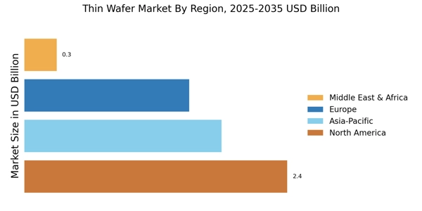
对研究和开发的投资增加是薄晶圆市场的推动力。随着公司努力创新和提升产品供应, substantial resources are being allocated to the development of new materials and processes. 这种对研发的关注对于提升薄晶圆的能力至关重要,使得能够生产出性能和效率更高的设备。预计到2025年,半导体研发支出将超过700亿美元,反映出行业对创新的承诺。这些投资可能会带来突破,进一步推动薄晶圆市场的发展,因为制造商寻求在不断发展的技术环境中保持竞争力。
With 5+ years of expertise in Market Intelligence and Strategic Research, Nirmit Biswas specializes in ICT, Semiconductors, and BFSI. Backed by an MBA in Financial Services and a Computer Science foundation, Nirmit blends technical depth with business acumen. He has successfully led 100+ projects for global enterprises and startups, including Amazon, Cisco, L&T and Huawei, delivering market estimations, competitive benchmarking, and GTM strategies. His focus lies in transforming complex data into clear, actionable insights that drive growth, innovation, and investment decisions. Recognized for bridging engineering innovation with executive strategy, Nirmit helps businesses navigate dynamic markets with confidence.
read more
Co-Author
Shubham Munde
Team Lead - Research
Shubham brings over 7 years of expertise in Market Intelligence and Strategic Consulting, with a strong focus on the Automotive, Aerospace, and Defense sectors. Backed by a solid foundation in semiconductors, electronics, and software, he has successfully delivered high-impact syndicated and custom research on a global scale. His core strengths include market sizing, forecasting, competitive intelligence, consumer insights, and supply chain mapping. Widely recognized for developing scalable growth strategies, Shubham empowers clients to navigate complex markets and achieve a lasting competitive edge. Trusted by start-ups and Fortune 500 companies alike, he consistently converts challenges into strategic opportunities that drive sustainable growth.
The secondary research process involved comprehensive analysis of semiconductor industry databases, peer-reviewed engineering journals, technical publications, and authoritative technology organizations. Key sources included the US Department of Commerce (Bureau of Industry and Security), European Semiconductor Industry Association (ESIA), SEMI (Semiconductor Equipment and Materials International), Institute of Electrical and Electronics Engineers (IEEE), Japan Electronics and Information Technology Industries Association (JEITA), Korea Semiconductor Industry Association (KSIA), China Semiconductor Industry Association (CSIA), National Institute of Standards and Technology (NIST), International Technology Roadmap for Semiconductors (ITRS), US Census Bureau - Manufacturing & Construction Division, Organisation for Economic Co-operation and Development (OECD) - STI Statistics, World Semiconductor Trade Statistics (WSTS), International Data Corporation (IDC), Gartner Semiconductor Research, European Commission - Digital Economy Reports, and national ministry reports from key semiconductor manufacturing markets including Taiwan Ministry of Economic Affairs (MOEA), Singapore Economic Development Board (EDB), and Ministry of Electronics and Information Technology (MeitY) - India. These sources were used to collect wafer production statistics, trade data, technology node migration trends, fab capacity utilization rates, and market landscape analysis for silicon, gallium arsenide, silicon carbide, and other compound semiconductor wafer technologies.
Primary Research
In order to gather both qualitative and quantitative insights, supply-side and demand-side stakeholders were interviewed during the primary research process. CEOs, VPs of Manufacturing Operations, CTOs of Advanced Packaging, heads of R&D, and business unit directors from semiconductor equipment OEMs, silicon foundries, and thin wafer makers were among the supply-side sources. Demand-side sources included supply chain managers from consumer electronics and automotive OEMs, procurement heads from fabless semiconductor businesses, fab directors from top foundries, and VP-level executives from IDMs (Integrated Device Manufacturers). Primary research obtained information on wafer thinning adoption trends, price dynamics, and supply chain localization tactics. It also verified technology migration timetables and validated market segmentation across thickness categories.
Primary Respondent Breakdown:
By Designation: C-level Primaries (28%), Director Level (32%), Others (40%)
By Region: North America (32%), Europe (30%), Asia-Pacific (33%), Rest of World (5%)
Market Size Estimation
Global market valuation was derived through revenue mapping and production volume analysis. The methodology included:
Identification of 50+ key manufacturers and foundry partners across North America, Europe, Asia-Pacific, and emerging semiconductor hubs
Product mapping across silicon, gallium arsenide, silicon carbide, and other compound semiconductor material categories
Analysis of reported and modeled annual revenues specific to thin wafer (≤300 micrometers) product portfolios
Coverage of manufacturers and foundry relationships representing 75-80% of global thin wafer market share in 2024
Extrapolation using bottom-up (wafer area shipment volume × ASP by region and thickness category) and top-down (manufacturer revenue validation) approaches to derive segment-specific valuations across semiconductor devices, optoelectronics, and MEMS applications
“This is really good guys. Excellent work on a tight deadline. I will continue to use you going forward and recommend you to others. Nice job”
Noah MalgeriCo-Founder
“Thanks. It’s been a pleasure working with you, please use me as reference with any other Intel employees.”
Joseph AguayoSales Operations & Pricing Manager
“Thanks for sending the report it gives us a good global view of the Betaïne market.”
Peter Groot koerkampAccount and Business Manager
“Thank you, this will be very helpful for OQS.”
La Terria DoddProgram Support Specialist
“We found the report very insightful! we found your research firm very helpful. I'm sending this email to secure our future business.”
Younghwan ChoiSenior Retail Manager
“I am very pleased with how market segments have been defined in a relevant way for my purposes (such as "Portable Freezers & refrigerators" and "last-mile").
In general the report is well structured. Thanks very much for your efforts.”
Mark IrwinManagement Consultant
“I have been reading the first document or the study, ,the Global HVAC and FP market report 2021 till 2026. Must say, good info! I have not gone in depth at all parts, but got a good indication of the data inside!”
Rob KooikerGroup Product Manager HVAC & Fire Protection GMA
“We got the report in time, we really thank you for your support in this process. I also thank to all of your team as they did a great job.”
Akif MorogluStrategy & Business Development Director
“The Automotive 48V ECU Components Procurement Intelligence Study” was a complex project, but the Market Research Future (MRFR) team handled it with quality, agility, and customer-centricity. They delivered all requested data on time and within the agreed scope. The team, including Shubhendra Anand and Rahul Gotadki, was always readily available to clarify questions and swiftly implement necessary adjustments, driving the project to a successful conclusion within a very demanding timeframe.
I would also like to specifically commend Akshay Agarwal for his responsiveness and support at every stage—from our initial inquiry on May 6th through to final delivery on June 18th. His dedication made the entire process seamless.”
Guilherme Gomes MartinsProduct Management Director