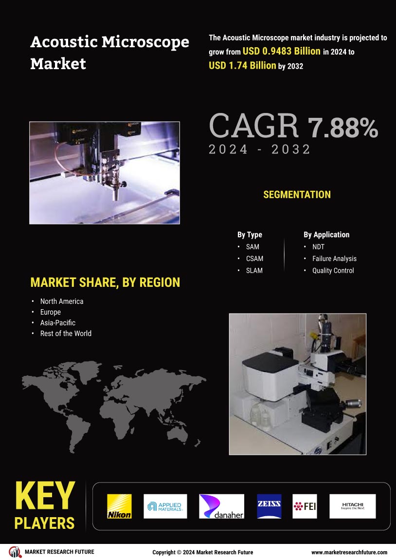
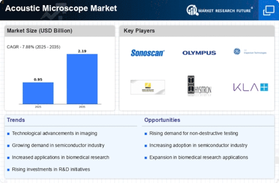
Leading market players are investing heavily in research and development to expand their product lines, which will help the acoustic microscope market grow even more. There are some strategies for action that market participants are implementing to increase their presence around the world's global footprint, with important market developments including new product launches, contractual agreements and acquisitions, higher investments, and collaboration with other organizations. To expand and survive in a more competitive and rising market climate, the acoustic microscope industry must offer cost-effective items.
Manufacturing locally to minimize operational costs is one of the key business tactics manufacturer use in the global acoustic microscope industry to benefit clients and increase the market sector. In recent years, the acoustic microscope industry has offered some of the most significant technological advancements. Major players in the acoustic microscope market, including Nikon Corporation, Applied Materials Inc, Danaher Corporation, Carl Zeiss, FEI Co., Hitachi High Technologies Corporation, Bruker Optics Inc, JEOL Ltd, Leica Microsystems, Olympus Corporation, and others, are attempting to grow market demand by investing in research and development operations.
Applied Materials Inc generates practically every new chip and advanced display globally, and our materials engineering solutions are the industry standard. Our atomic-level and industrial-scale material modification expertise helps our clients make the impossible possible.
In July Applied Materials, Inc. unveiled new materials, methods, and systems that facilitate chipmakers' use of hybrid bonding and through-silicon vias (TSVs) to integrate chipsets into cutting-edge 2.5D and 3D packaging. Applied's new solutions for heterogeneous integration (HI) increase the company's extensive portfolio of HI technologies.
Using innovative packaging techniques, HI assists semiconductor businesses in fusing chipsets with different functions, technological nodes, and sizes to as a unified whole. The exponential growth in demand for transistors in applications like high-performance computing and artificial intelligence, coupled with the diminishing and increasingly costly ability to shrink transistors using traditional 2D scaling, presents significant challenges for the electronics industry, which HI helps addressed specimens and cells because of the increased accuracy with which their true colors may be displayed.
Hitachi High-Tech, with headquarters in Tokyo, Japan, produces and sells clinical analyzers, biotechnology goods, analytical instruments, semiconductor production equipment, and analysis equipment, as well as offering solutions with a high added value for transportation, social infrastructure, etc.
In January Hitachi High-Tech Corporation introduced the AFM100 Pro High-Sensitivity Scanning Probe Microscope System, a high-end scanning probe microscope (AFM*1/SPM*2) featuring a newly developed high-sensitivity optical head that increases sensitivity when measuring physical properties and enables measurement at atomic and molecular scales. Highly sensitive measuring and analysis equipment is in high demand in the research and development of new functional materials.The AFM100 Pro can be used for on-site analysis. Thus it can help with customer problems.
