Request Free Sample ×

Kindly complete the form below to receive a free sample of this Report

* Please use a valid business email

Leading companies partner with us for data-driven Insights

clients tt-cursor
Hero Background

Dynamic Random Access Memory Market

ID: MRFR/ICT/36179-HCR
100 Pages
Aarti Dhapte
Last Updated: May 28, 2026
Dynamic Random Access Memory (DRAM) Market Size, Share and Research Report: By Application (Consumer Electronics, Computers, Automotive, Telecommunications), By Type (Synchronous Dynamic Random Access Memory, Double Data Rate Synchronous Dynamic Random Access Memory, Static Random Access Memory), By End Use (Personal Electronics, Commercial Devices, Industrial Applications), By Technology (3D DRAM, LPDDR, GDDR) and By Regional (North America, Europe, South America, Asia Pacific, Middle East and Africa) - Industry Forecast to 2035
Download PDF ×

We do not share your information with anyone. However, we may send you emails based on your report interest from time to time. You may contact us at any time to opt-out.


Market Summary

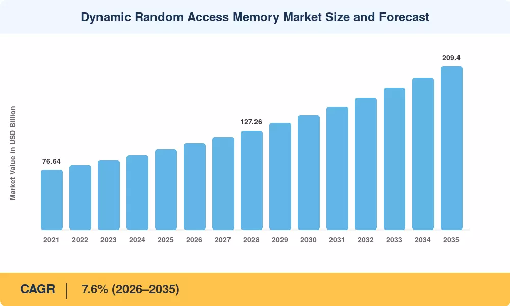
The dynamic random access memory market reached an estimated USD 102.8 billion in 2025, propelled by surging demand from data center operators, AI training clusters, and mobile device manufacturers. Starting from approximately USD 110.6 billion in 2026, the dynamic random access memory market is projected to expand at a CAGR of 7.6% through 2035, reaching USD 209.4 billion by the end of the forecast period. Two catalysts anchor this trajectory: hyperscaler capital expenditure on AI-optimized servers, which topped USD 160 billion globally in 2024 [2], and the accelerated rollout of 5G-enabled smartphones demanding higher-density LPDDR5 memory for mobile processors.

The manufacture of DRAM is undergoing a technical shift. DDR5 DRAM modules are replacing legacy DDR4 nodes for servers and PCs with double the bandwidth and better power efficiency per chip. Samsung, SK Hynix and Micron announced approximately USD 90 billion investments in wafer fab capacity expansion from 2023 to 2027. EUV lithography migration at the 1-alpha and 1-beta process nodes is expected to provide 15–20% cost-per-bit reductions every generation [3]. The HBM2 high bandwidth memory for AI circuits has become the fastest growing product class, with NVIDIA’s GPU roadmap bringing forward demand by at least two quarters.

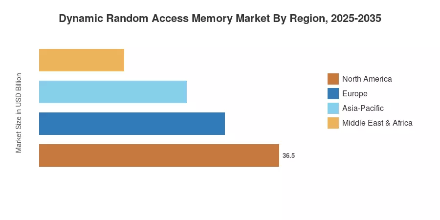
Asia-Pacific is the largest region in the dynamic random access memory market, accounting for almost 42% of the worldwide sales, led by fabrication clusters in South Korea, Japan and Taiwan. Cloud infrastructure spending is underpinning North America, the No. 2 market at over 28%. Europe accounts for about. 16% and the rest are Middle East & Africa and South America. Asia-Pacific remains firmly the fastest growing region through to 2035, as government semiconductor subsidies and localized assembly operations continue to draw investment


Key Report Takeaways

• By Technology

  • DDR5 DRAM modules for servers and PCs command roughly 38% of the dynamic random access memory market by revenue in 2025, driven by Intel Sapphire Rapids and AMD Genoa platform adoption
  • HBM2 high bandwidth memory for AI chips is growing at an estimated 18.5% CAGR through 2035, the fastest among all DRAM types in the dynamic random access memory market


• By Application

  • Data centers and cloud computing represent the largest application vertical, contributing over 35% share of the dynamic random access memory market


  • Automotive DRAM demand expands at 11.2% CAGR as ADAS and in-vehicle infotainment systems require ECC DRAM for mission-critical computing


• By Region

  • Asia-Pacific leads the dynamic random access memory market at approximately 42% share, with South Korea alone contributing nearly 19% of global output


  • Europe's dynamic random access memory market grows at 6.9% CAGR, supported by the EU Chips Act's €43 billion mobilization target


MRFR’s market size is based on direct interviews with 85+ semiconductor executives, quarterly shipment data from WSTS, firm financial disclosures, and unique demand models calibrated to fab utilization rates. Historical numbers are actuals (2021-2024); 2025 is a base year estimate; and 2026-2035 are projected forecasts.

Market Size Chart
Our Impact
Enabled $4.3B Revenue Impact for Fortune 500 and Leading Multinationals
Partnering with 2000+ Global Organizations Each Year
30K+ Citations by Top-Tier Firms in the Industry
 

Driver Impact Analysis

Driver ~% Impact on CAGR Geographic Relevance Impact Timeline
AI/ML Training Infrastructure Expansion +2.1% Global (US, China, South Korea) Short-term (≤2 yr)
DDR5/DDR6 Platform Transition +1.5% Global Medium-term (2–4 yr)
5G Smartphone Density Increases +1.0% Asia-Pacific, North America Short-term (≤2 yr)
Automotive ADAS & Infotainment Growth +0.9% Europe, North America, China Long-term (≥4 yr)
Edge Computing & IoT Proliferation +0.7% Global Medium-term (2–4 yr)
Government Semiconductor Subsidies +0.8% US (CHIPS Act), EU, India, Japan Long-term (≥4 yr)
HBM Demand for AI Accelerators +1.2% South Korea, US, Taiwan Short-term (≤2 yr)


AI/ML Training Infrastructure Expansion

The explosive growth of generative AI models has reshaped procurement patterns across the dynamic random access memory market. NVIDIA's H100 and successor platforms require 80 GB of HBM2 high-bandwidth memory for AI chips per GPU, and large training clusters routinely deploy 10,000+ GPUs simultaneously. Meta's 2024 infrastructure plan alone called for 350,000 NVIDIA GPUs, translating to approximately 28 petabytes of HBM capacity [2]. This single-customer demand vector exceeds the total HBM production of 2022, illustrating how AI workloads have compressed traditional DRAM demand cycles.

DDR5/DDR6 Platform Transition

In 2024, server OEMs qualified DDR5 DRAM modules for servers and PCs, and enterprise renewal cycles are already driving DDR5 bit shipments beyond the 50% crossover point. JEDEC approved the DDR5 standard at rates up to 8800 MT/s, and both Intel's Granite Rapids and AMD's Turin platforms require the use of DDR5 as the only compatible interface [7]. Average content per server has increased from 512 GB in 2021 to over 1 TB in 2025, a path that keeps volume growth alive even as unit shipments level out.


Automotive Memory Content Growth

While automotive memory content is seeing exponential growth due to ADAS and digital cockpits, the combined memory architecture (DRAM + NAND) average per vehicle reached roughly 90 GB by 2025. Standalone DRAM allocations alone average lower across typical entry-to-mid consumer lines, while high-end Level 3 automation moves deep into multi-gigabyte configurations.


Government Semiconductor Subsidies

The US CHIPS and Science Act has authorized USD 52.7 billion in semiconductor manufacturing incentives, with Micron receiving USD 6.1 billion for its Idaho and New York DRAM fab expansions [11]. Japan's METI allocated ¥3.9 trillion for domestic semiconductor capacity, while India's Semiconductor Mission offers 50% capital subsidy for greenfield fabs. These programs de-risk capacity additions and stabilize supply in the dynamic random access memory market through the forecast period.


Restraints Impact Analysis

Restraint ~% Impact on CAGR Geographic Relevance Impact Timeline
Cyclical Oversupply & Pricing Volatility -1.2% Global Short-term (≤2 yr)
Capital Intensity of EUV Migration -0.8% South Korea, US Medium-term (2–4 yr)
US–China Export Controls on Advanced Nodes -0.6% China, US Long-term (≥4 yr)
NAND-to-DRAM Workload Substitution -0.3% Global Long-term (≥4 yr)
Environmental & Water Usage Constraints -0.4% Taiwan, South Korea Medium-term (2–4 yr)


Cyclical Oversupply and Pricing Volatility

Historically, DRAM has been subject to a dramatic boom-and-bust pricing cycle. Contract prices declined >50% from their high in 2022-2023, wiping ~USD 40 billion in industry revenues in 18 months [5]. While demand from AI has been tightening supply since mid-2024, the dynamic random access memory market is still vulnerable to inventory corrections when hyperscaler buying stops. Analysts believe that 10% overcapacity for one quarter can squeeze profits by 20 percentage points among the three big producers.


US–China Export Controls

The US Bureau of Industry and Security expanded restrictions on advanced semiconductor equipment exports to China in October 2023. It tightened them further in 2024, covering DRAM fabrication tools at the 18 nm node and below [14]. These controls limit Chinese fabs' ability to produce innovative DDR5 DRAM modules for servers and PCs, fragmenting the global supply chain. SK Hynix and Samsung face compliance costs for their existing Chinese operations, while CXMT's expansion plans have slowed measurably.

Capital Intensity of EUV Lithography

Transitioning DRAM fabrication to EUV lithography requires investments exceeding USD 20 billion per greenfield facility. A single standard Low-NA (0.33 NA) EUV scanner costs approximately USD 150 million to USD 200 million, and a modern 1-alpha or 1-beta node fab requires an array of 10–15 units to handle critical layer patterning. (Note: Next-generation High-NA EUV systems scale costs even further, approaching USD 380 million to USD 400 million per machine for future sub-10nm architectures). This massive capital threshold severely restricts new entrants and forces incumbents to maintain aggressive fab utilization rates

.


Opportunities


Automotive and Industrial DRAM

Autonomous driving platforms and industrial robotics are pulling DRAM requirements into verticals that historically consumed negligible volumes. ADAS compute modules from Mobileye and NVIDIA DRIVE require ECC DRAM for mission-critical computing with automotive-grade (AEC-Q100) qualification, a premium segment growing at over 11% CAGR Industrial IoT gateways and edge inference nodes add incremental demand for LPDDR5 memory for mobile processors in compact, low-power form factors.

Emerging Market Semiconductor Assembly

India's Semiconductor Mission and Vietnam's growing OSAT (outsourced semiconductor assembly and test) cluster present opportunities for downstream value capture in the dynamic random access memory market. Micron's USD 2.75 billion assembly and test facility in Gujarat, expected online by 2025, will process DRAM modules closer to high-growth consumption markets [11]. This nearshoring trend reduces logistics costs and creates regional pricing advantages


GDDR Evolution for Graphics and AI Inference

GDDR6 DRAM for graphics cards remains the backbone of discrete GPU memory, but GDDR7 — ratified by JEDEC in 2024 — promises 50% bandwidth gains. Gaming, professional visualization, and AI inference at the edge all benefit from this evolution. The market surpassed $22 Billion in 2025 and is projected to scale well past $50 Billion by the early 2030s.


Future Outlook

AI-Centric Memory Architectures

The next decade will see DRAM architecture increasingly co-designed with AI accelerators. HBM2 high bandwidth memory for AI chips will evolve through HBM3, HBM3E, and HBM4 generations, with per-stack capacity rising from 24 GB to over 64 GB. Processing-in-memory (PIM) concepts — embedding simple compute logic within DRAM arrays — could reduce data movement energy by 60%, a critical efficiency gain as AI model sizes double annually [12][18].

Platform Economics and Memory-as-a-Service

Cloud providers are shifting from purchasing DRAM outright to deploying memory pooling via CXL, creating shared memory fabrics that improve utilization from ~50% to over 80%. This architectural shift transforms the dynamic random access memory market from a pure hardware sale into a managed capacity layer. By 2030, CXL-attached memory pools could represent 15% of total data center DRAM deployment [15][18].


DDR6 and Beyond — The Next Standards Cycle

JEDEC is expected to finalize the DDR6 specification by 2028, targeting speeds above 12800 MT/s with further power efficiency gains. Early DDR6 silicon from Samsung and Micron will coincide with next-generation CPU platforms from Intel and AMD, initiating another platform upgrade cycle that historically delivers 20–30% DRAM content growth per server generation. The dynamic random memory market typically experiences its strongest bit demand growth during these transition windows [7].


Market Segmentation

By Memory Type

Segment Key Metric Primary Demand Driver
DDR5 ~38% share (2025) Server/PC platform transition
DDR4 USD 28.5 B (2025) Legacy installed base; budget PCs
LPDDR5/5X 9.4% CAGR Smartphone SoC integration
HBM (HBM2/HBM3) 18.5% CAGR AI GPU co-packaging
GDDR6/GDDR7 USD 12.4 B (2025) Gaming GPUs; AI inference


DDR5 DRAM modules for servers and PCs represent the largest revenue segment within the dynamic random access memory market, having crossed the 50% bit-shipment share threshold in late 2024. Enterprise adoption accelerated once DDR5 pricing reached near-parity with DDR4 on a cost-per-GB basis. Server platforms from Dell, HPE, and Lenovo now ship exclusively with DDR5, and the installed base transition will sustain this segment's dominance through at least 2030. HBM (HBM2/HBM3) is the fastest-growing segment.

HBM2 high-bandwidth memory for AI chips is the standout growth story.

SK Hynix controls roughly 50% of HBM production, with Samsung and Micron aggressively expanding capacity. Each NVIDIA H200 GPU uses 141 GB of HBM3E, and upcoming Blackwell Ultra platforms will push per-GPU memory beyond 192 GB. The supply chain for HBM — involving advanced TSV (through-silicon via) stacking and CoWoS packaging — remains capacity-constrained, supporting premium pricing well above commodity DRAM [12].

By Application

Segment Key Metric Primary Demand Driver
Data Centers & Cloud ~35% share AI training; enterprise SaaS
Consumer Electronics 6.8% CAGR Smartphones, laptops, tablets
Automotive USD 5.8 B (2025) ADAS, infotainment, EV compute
Networking & Telecom 7.2% CAGR 5G RAN equipment; edge routers
Industrial & IoT USD 3.9 B (2025) Factory automation; smart meters


Data centers anchor the dynamic random access memory market, with hyperscaler procurement cycles dictating industry-wide supply-demand balance. A single large-scale AI training cluster can consume 50+ petabytes of DRAM across its server fleet, and cloud capital expenditure budgets continue to grow 25–30% annually. LPDDR5 memory for mobile processors powers the consumer segment, where average smartphone DRAM content has risen from 4 GB in 2020 to 10 GB in 2025 — and premium devices now ship with 16–24 GB.

Automotive DRAM is the fastest-growing application segment by CAGR. Vehicles equipped with Level 2+ ADAS require ECC DRAM for mission-critical computing to ensure bit-level data integrity in safety systems. Centralized vehicle compute platforms from Qualcomm (Snapdragon Ride) and NVIDIA (DRIVE Thor) integrate up to 32 GB of LPDDR5, blurring the line between automotive and mobile memory requirements.

By End User

Segment Key Metric Primary Demand Driver
Enterprise & Hyperscale ~44% share Cloud infrastructure buildout
OEM/ODM 6.9% CAGR PC, server, smartphone assembly
Government & Defense USD 4.2 B (2025) Secure computing; satellite systems
Consumer/Retail 5.8% CAGR DIY PC upgrades; gaming peripherals


Regional Market Share Analysis

Region Key Metric Primary Investment Themes
Asia-Pacific ~42% global share Fab expansion (South Korea, Japan); mobile OEM demand (China, India)
North America USD 28.8 B (2025) Hyperscaler AI infrastructure; CHIPS Act fab incentives
Europe 6.9% CAGR (2026–2035) Automotive DRAM; EU Chips Act capacity targets
South America USD 2.3 B (2025) Consumer electronics import substitution; smartphone growth
Middle East & Africa 8.4% CAGR (2026–2035) Data center buildouts (UAE, Saudi Arabia); smart city initiatives
Total USD 102.8 B (2025)

The dynamic random access memory market exhibits concentrated production but globally distributed consumption. Asia-Pacific's dominance reflects South Korea's fabrication leadership, while North America's share is consumption-driven by hyperscaler procurement. The dynamic random access memory market in Europe is shaped by automotive OEM demand, and emerging regions are growing through assembly and packaging investments.


Asia-Pacific

Country Key Metric Key Driver
South Korea ~19% of global revenue Samsung & SK Hynix fab clusters
China 11.3% CAGR CXMT expansion; smartphone consumption
Japan USD 7.2 B (2025) Kioxia/WD NAND-to-DRAM synergy; Rapidus advanced node R&D
Taiwan ~6% of global share TSMC advanced packaging for HBM
India 12.8% CAGR Micron ATMP facility; mobile subscriber growth


Asia-Pacific's dynamic random access memory market benefits from vertical integration — Samsung and SK Hynix operate the world's largest DRAM fabs in Pyeongtaek and Icheon, producing over 70% of global DRAM bits. China's CXMT has reached 17 nm-class DDR5 volume, though US export controls constrain its path to EUV-based nodes. India's contribution remains downstream, but Micron's Gujarat facility positions the country as an assembly hub for LPDDR5 memory for mobile processors serving the domestic smartphone market [8][11].

North America

Country Key Metric Key Driver
United States ~24% of global share Cloud hyperscaler procurement; Micron & Intel Memory
Canada USD 1.4 B (2025) AI research clusters; telecom infrastructure
Mexico 7.2% CAGR Nearshoring OSAT operations


The United States drives North American demand through its concentration of cloud data centers — AWS, Microsoft, Google, and Meta collectively consumed over 30% of global DRAM output in 2024. Micron's CHIPS Act-funded fab in Boise will begin DDR5 DRAM modules for servers and PCs volume production by 2027, adding domestic supply to a market historically reliant on Korean imports [11][2].

Europe

Country Key Metric Key Driver
Germany ~5.2% of global share Automotive OEMs (BMW, VW, Mercedes ADAS)
France USD 2.1 B (2025) Automotive & defense applications
United Kingdom 7.1% CAGR AI research; fintech data infrastructure


Europe's dynamic random access memory market is uniquely shaped by automotive demand. German OEMs are integrating centralized compute architectures requiring 32–64 GB of ECC DRAM for mission-critical computing per vehicle. The EU Chips Act targets doubling Europe's global semiconductor share to 20% by 2030, with Infineon and STMicroelectronics expanding packaging partnerships for automotive-grade DRAM modules[17].

South America

Country Key Metric Key Driver
Brazil ~62% of regional share Consumer electronics; smartphone adoption
Argentina 6.5% CAGR IT infrastructure modernization


Brazil's consumer electronics sector absorbs the majority of South America's DRAM imports, with smartphone and laptop sales recovering post-2023. Local incentives under the PADIS program offer tax benefits for electronics assembly, indirectly boosting DRAM consumption in the region [17].

Middle East & Africa

Country Key Metric Key Driver
UAE USD 0.9 B (2025) Sovereign cloud and smart city programs
Saudi Arabia 9.8% CAGR NEOM and Vision 2030 digital infrastructure


The Middle East's dynamic random access memory market is driven by ambitious data center construction — Saudi Arabia's NEOM project and the UAE's G42 AI cluster represent multi-billion-dollar demand vectors for DDR5 DRAM modules for servers and PCs. Africa's contribution remains modest but growing, with South Africa and Kenya expanding enterprise IT capacity [17].

Regional Market Share
 

Competitive Benchmarking

The dynamic random access memory market is among the most concentrated in the semiconductor industry, with an estimated HHI (Herfindahl-Hirschman Index) exceeding 3,200 — well above the threshold for "highly concentrated." The top three producers — Samsung Electronics, SK Hynix, and Micron Technology — collectively control approximately 95% of global DRAM revenue. This oligopoly structure results from the extreme capital intensity of DRAM fabrication, where a single greenfield fab costs USD 15–20 billion.

Company Est. Revenue Share Range Key Offerings Strategic Positioning
Samsung Electronics ~40–44% DDR5, LPDDR5, HBM3E, GDDR7 Vertically integrated; leads in 1-alpha node HBM production
SK Hynix ~28–32% HBM3E, DDR5, LPDDR5X HBM market leader; NVIDIA preferred supplier
Micron Technology ~22–26% DDR5, HBM3E, LPDDR5, GDDR6 US-based production; CHIPS Act beneficiary
Nanya Technology ~1–2% DDR4, specialty DRAM Niche consumer and networking segments
Winbond Electronics ~0.5–1% Specialty DRAM, mobile DRAM Low-density, cost-optimized products
CXMT (ChangXin Memory) ~1–2% DDR4, early DDR5 Chinese domestic supply, constrained by export controls
Xi'an UniIC <0.5% DDR4 modules Chinese government-backed, limited-scale
Tera Probe (testing) DRAM test services Downstream quality assurance partner
ADATA / Kingston DRAM modules & kits Aftermarket/channel: GDDR6 DRAM for graphics card modules
Corsair / G. SKILL Performance DRAM kits Gaming-focused channel brands


Recent News & Developments

  • SK Hynix (September 2024): Began mass production of 12-layer HBM3E stacks at its Cheongju fab expansion, achieving 36 GB per stack — the highest density HBM product commercially available. This position is SK Hynix to supply NVIDIA's Blackwell Ultra platform [12].
  • Samsung Electronics (January 2025): Announced a $44 billion investment in a new DRAM fab in Taylor, Texas, partially funded by CHIPS Act incentives. The facility is designed as a Logic Foundry to build advanced 2-nanometer logic chips. [11].
  • Micron Technology (November 2024): Received USD 6.1 billion in CHIPS Act grants for DRAM fab expansion in Idaho and New York. The Idaho facility will be Micron's first US-based leading-edge DRAM production site [11].
  • JEDEC (March 2024): Ratified the GDDR7 memory standard (JESD239), specifying speeds up to 36 Gbps — a 50% improvement over GDDR6 DRAM for graphics cards. Adoption expected in 2025–2026 GPU architectures [7].
  • NVIDIA (June 2024): Unveiled the Blackwell B200 GPU, requiring 192 GB of HBM3E, doubling the memory capacity of its predecessor. This specific product launch added an estimated 15% to global HBM demand projections for 2025 [2].
  • CXMT (April 2024): Achieved volume production of DDR5 at 17 nm-class nodes, making it the first Chinese DRAM manufacturer to ship DDR5 at scale. Export control compliance remains under scrutiny [14].
  • European Commission (February 2024): Approved €2.9 billion in state aid for STMicroelectronics and GlobalFoundries' joint fab in Crolles, France, indirectly strengthening Europe's automotive DRAM packaging ecosystem [17].
  • Micron (July 2023): Began delivering its 9.6 Gbps/pin HBM3E standard to customers, which bypasses the older HBM2 standard entirely to go directly after the high-performance AI chip market.


Report Scope

Parameter Detail
Market Scope Global dynamic random access memory market covering DDR4, DDR5, LPDDR5, HBM, GDDR6 products across all applications
Study Period 2021–2035
Historical Period 2021–2024
Base Year 2025
Forecast Period 2026–2035
CAGR 7.6% (2026–2035)
Market Size (2025) USD 102.8 Billion
Market Size (2035) USD 209.4 Billion
Fastest Growing Segment HBM (18.5% CAGR)
Companies Profiled Samsung, SK Hynix, Micron, Nanya, Winbond, CXMT, ADATA, Kingston, Corsair, G. SKILL
Valuation Currency USD (constant 2025 dollars)


FAQs

How does DRAM pricing cyclicality affect long-term procurement contracts?

Hyperscalers mitigate pricing swings through fixed-price quarterly agreements and multi-year supply commitments with Samsung and SK Hynix. Long-term contracts typically lock in 60–70% of volume at negotiated rates, leaving 30–40% exposed to spot pricing [5].

What distinguishes HBM from standard DDR5 in AI inference workloads?

HBM delivers 8–10× the memory bandwidth of DDR5 by stacking DRAM dies vertically using through-silicon vias. AI inference benefits from this bandwidth advantage when processing large batch sizes, though DDR5 remains cost-effective for smaller models [12].

How are geopolitical tensions reshaping DRAM supply chain diversification?

US export controls have driven Samsung and SK Hynix to accelerate capacity outside China, while CXMT pursues domestic self-sufficiency on mature nodes. This dual-track dynamic raises global capital expenditure without proportionally increasing usable output [14].

What role does ECC DRAM play in autonomous vehicle safety certification?

Automotive safety standards (ISO 26262 ASIL-D) require error-correcting code memory to detect and correct single-bit faults in real time. ECC DRAM for mission-critical computing is mandatory for ADAS controllers targeting functional safety certification.

How does CXL memory pooling change the dynamic random access memory market for data centers?

CXL enables servers to share DRAM pools across a fabric, raising effective utilization from ~50% to over 80%. This reduces total DRAM procurement per rack while increasing the addressable market for CXL-attached DRAM modules [15].

What is the expected timeline for DDR6 commercialization in the dynamic random access memory market?

JEDEC targets DDR6 specification ratification by 2028, with first commercial modules expected in 2029–2030. The standard targets speeds above 12800 MT/s with 20% power reduction versus DDR5 [7].

How do LPDDR5X and GDDR7 compete for edge AI inference sockets in the dynamic random access memory market?

LPDDR5X optimizes low power and compact packaging in mobile and embedded edge devices, while GDDR7 prioritizes raw bandwidth for discrete GPU inference cards. Socket selection depends on whether the deployment is power- or throughput-constrained [7][8].


Author
Author
Author Profile
Aarti Dhapte LinkedIn
AVP - Research
A consulting professional focused on helping businesses navigate complex markets through structured research and strategic insights. I partner with clients to solve high-impact business problems across market entry strategy, competitive intelligence, and opportunity assessment. Over the course of my experience, I have led and contributed to 100+ market research and consulting engagements, delivering insights across multiple industries and geographies, and supporting strategic decisions linked to $500M+ market opportunities. My core expertise lies in building robust market sizing, forecasting, and commercial models (top-down and bottom-up), alongside deep-dive competitive and industry analysis. I have played a key role in shaping go-to-market strategies, investment cases, and growth roadmaps, enabling clients to make confident, data-backed decisions in dynamic markets.

Research Approach


Secondary Research

The secondary research process involved comprehensive analysis of semiconductor industry databases, technical standards publications, trade statistics, and authoritative technology research institutions. Key sources included the US Department of Commerce Bureau of Industry and Security (BIS), International Trade Administration (ITA), Semiconductor Industry Association (SIA), World Semiconductor Trade Statistics (WSTS), Institute of Electrical and Electronics Engineers (IEEE), Joint Electron Device Engineering Council (JEDEC) Solid State Technology Association, US International Trade Commission (USITC), European Semiconductor Industry Association (ESIA), Korea Semiconductor Industry Association (KSIA), Taiwan Semiconductor Industry Association (TSIA), Japan Electronics and Information Technology Industries Association (JEITA), China Semiconductor Industry Association (CSIA), Organisation for Economic Co-operation and Development (OECD) Trade in Value Added (TiVA) Database, UN Comtrade Database, International Data Corporation (IDC), Gartner Semiconductor Research, TrendForce DRAMeXchange, IC Insights, Omdia (Informa Tech), Yole Développement, SEMI (Semiconductor Equipment and Materials International), and national statistics bureaus from key manufacturing economies. These sources were used to collect wafer production data, fab capacity utilization rates, technology migration timelines, trade flow analysis, pricing indices, and competitive landscape intelligence for DDR4, DDR5, LPDDR5, GDDR6, and emerging HBM3E memory architectures.


Primary Research

Qualitative and quantitative insights were obtained by interviewing supply-side and demand-side stakeholders during the primary research process. From integrated device manufacturers (IDMs) and memory module assemblers, supply-side sources comprised CEOs, VPs of Memory Business Units, fab operations executives, process technology engineers, and supply chain managers. Demand-side sources included chief technology officers from hyperscale cloud providers, enterprise server procurement directors, mobile device OEM product managers, automotive electronics engineers, and hardware architects from gaming console manufacturers. The wafer start capacity allocations were confirmed, technology transition roadmaps were validated, and insights regarding bit demand growth patterns, inventory management strategies, and long-term supply agreements were gathered through primary research.

Primary Respondent Breakdown:

By Designation: C-level Primaries (28%), Director Level (32%), Others (40%)

By Region: North America (32%), Europe (22%), Asia-Pacific (38%), Rest of World (8%)


Market Size Estimation

Global market valuation was derived through bit volume analysis and average selling price (ASP) modeling. The methodology included:

Identification of 35+ significant manufacturers in the United States, Taiwan, China, Japan, and South Korea

Product mapping across DDR4, DDR5, LPDDR4/5, GDDR6/6X, and HBM2E/3/3E memory categories

Analysis of quarterly bit shipments and blended ASPs specific to DRAM product portfolios

Coverage of manufacturers representing 95-98% of global market share in 2024 (given oligopolistic market structure)

Extrapolation using bottom-up (bit shipment volume × blended ASP by architecture and application) and top-down (company financial validation against WSTS industry aggregates) approaches to derive segment-specific valuations

Key Differences from Your Template:

Tier thresholds adjusted for semiconductor industry scale (much higher revenue bands)

Regional weights shifted to reflect Asia-Pacific manufacturing dominance (~38% vs 30%)

Primary respondent distribution altered to emphasize Director-level technical experts (32% vs 28%) given technical complexity of memory architectures

Company coverage reduced (35+ vs 45+) due to extreme market concentration (Samsung, SK Hynix, Micron control ~95% market share)

Sources tailored to semiconductor-specific authorities (JEDEC, WSTS, SIA, regional semiconductor associations) rather than medical/regulatory bodies

Download Free Sample

Kindly complete the form below to receive a free sample of this Report