×
Request Free Sample ×

Kindly complete the form below to receive a free sample of this Report

* Please use a valid business email

Leading companies partner with us for data-driven Insights

clients tt-cursor
Hero Background

GaAs Wafer Market

ID: MRFR/SEM/5011-HCR
100 Pages
Aarti Dhapte
October 2025

GaAs Wafer Market Research Report Information By Production Method (Vertical Gradient Freeze (VGF), Liquid Encapsulated Czochralski (LEC), Molecular Beam Epitaxy (MBE), and Metal Organic Vapor Phase Epitaxy (MOVPE)), By Applications (Mobile Device, Photovoltaic Devices, Wireless Communication, Optoelectronic Device, Aerospace & Defense, and Others) And By Region (North America, Europe, Asia-Pacific, And Rest Of The World) –Industry Forecast Till 2035

Share:
Download PDF ×

We do not share your information with anyone. However, we may send you emails based on your report interest from time to time. You may contact us at any time to opt-out.

GaAs Wafer Market Infographic
Purchase Options

GaAs Wafer Market Summary

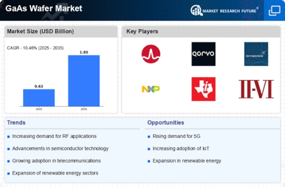
As per MRFR analysis, the GaAs Wafer Market Size was estimated at 0.62 USD Billion in 2024. The GaAs Wafer industry is projected to grow from 0.6849 in 2025 to 1.852 by 2035, exhibiting a compound annual growth rate (CAGR) of 10.46 during the forecast period 2025 - 2035.

Key Market Trends & Highlights

The GaAs Wafer Market is poised for substantial growth driven by technological advancements and increasing demand across various sectors.

  • North America remains the largest market for GaAs wafers, driven by robust telecommunications infrastructure.
  • Asia-Pacific is emerging as the fastest-growing region, fueled by rapid advancements in consumer electronics.
  • The Vertical Gradient Freeze segment dominates the market, while the Metal Organic Vapor Phase Epitaxy segment is witnessing the fastest growth.
  • Technological advancements and rising demand in telecommunications are key drivers propelling the GaAs wafer market forward.

Market Size & Forecast

2024 Market Size 0.62 (USD Billion)
2035 Market Size 1.852 (USD Billion)
CAGR (2025 - 2035) 10.46%

Major Players

Broadcom (US), Qorvo (US), Skyworks Solutions (US), NXP Semiconductors (NL), Texas Instruments (US), II-VI Incorporated (US), Aixtron SE (DE), Sumitomo Electric Industries (JP), Mitsubishi Chemical Corporation (JP)

GaAs Wafer Market Trends

The GaAs Wafer Market is currently experiencing a dynamic evolution, driven by advancements in technology and increasing demand across various sectors. The proliferation of consumer electronics, particularly smartphones and tablets, has led to a heightened need for high-performance semiconductor materials. Gallium arsenide, known for its superior electron mobility and efficiency, is becoming increasingly favored over traditional silicon in applications such as RF devices and optoelectronics. This shift suggests a potential for growth as manufacturers seek to enhance device performance and energy efficiency. Moreover, the GaAs Wafer Market is likely to benefit from the ongoing expansion of the telecommunications sector, particularly with the rollout of next-generation networks. The demand for faster and more reliable communication systems appears to be a driving force behind the increased utilization of GaAs wafers in the production of high-frequency components. As industries continue to innovate and integrate advanced technologies, the market for GaAs wafers may witness further diversification, catering to emerging applications in automotive, aerospace, and renewable energy sectors. This multifaceted growth trajectory indicates a promising outlook for stakeholders in the GaAs Wafer Market.

Technological Advancements

Recent innovations in fabrication techniques are enhancing the quality and performance of GaAs wafers. These advancements enable the production of thinner and more efficient wafers, which could lead to improved device performance in various applications.

Rising Demand in Telecommunications

The ongoing expansion of telecommunications infrastructure, particularly with the advent of next-generation networks, is driving the need for high-frequency components. GaAs wafers are increasingly utilized in the development of these components, suggesting a robust market demand.

Emerging Applications

The GaAs Wafer Market is witnessing diversification as new applications emerge in sectors such as automotive and renewable energy. This trend indicates a potential for growth as industries seek to leverage the unique properties of GaAs in innovative ways.

GaAs Wafer Market Drivers

Rising Demand in Telecommunications

The telecommunications sector is a significant driver for the GaAs Wafer Market, as the demand for high-speed data transmission continues to escalate. With the rollout of 5G networks, the need for advanced semiconductor materials, including GaAs wafers, is becoming increasingly critical. GaAs wafers are favored for their superior electron mobility and efficiency, making them ideal for high-frequency applications such as RF and microwave devices. The telecommunications industry is expected to invest heavily in upgrading infrastructure, which could lead to a substantial increase in GaAs wafer consumption. Analysts estimate that the telecommunications segment could account for over 30% of the total GaAs wafer market by 2026, underscoring the material's pivotal role in the evolution of communication technologies.

Growth in Renewable Energy Technologies

The GaAs Wafer Market is also being propelled by the growth in renewable energy technologies, particularly in solar energy applications. GaAs-based solar cells are recognized for their high efficiency and performance, making them suitable for both terrestrial and space applications. As the world increasingly shifts towards sustainable energy solutions, the demand for GaAs wafers in photovoltaic systems is expected to rise. Current projections indicate that the market for GaAs solar cells could expand by over 20% in the next few years, driven by advancements in solar technology and government incentives for renewable energy adoption. This trend highlights the potential for the GaAs Wafer Market to play a crucial role in the transition to cleaner energy sources.

Emerging Applications in Consumer Electronics

The GaAs Wafer Market is witnessing a notable expansion due to emerging applications in consumer electronics. As devices become more sophisticated, the demand for high-performance components is rising. GaAs wafers are increasingly utilized in smartphones, tablets, and other portable devices, where their lightweight and efficient properties are advantageous. The market for consumer electronics is projected to grow significantly, with estimates suggesting a potential increase of 15% in GaAs wafer usage within this sector by 2025. This trend indicates a shift towards more advanced materials that can support the growing functionalities of modern devices. Consequently, the GaAs Wafer Market is likely to benefit from this burgeoning demand, leading to innovations and enhancements in product offerings.

Technological Advancements in GaAs Wafer Market

The GaAs Wafer Market is experiencing a surge in technological advancements that enhance the performance and efficiency of semiconductor devices. Innovations in fabrication techniques, such as molecular beam epitaxy and metal-organic chemical vapor deposition, are enabling the production of high-quality GaAs wafers with improved electrical properties. These advancements are crucial for applications in high-frequency and high-power electronics, which are increasingly in demand. The market for GaAs wafers is projected to grow at a compound annual growth rate of approximately 10% over the next five years, driven by the need for faster and more efficient electronic components. As technology continues to evolve, the GaAs Wafer Market is likely to witness further enhancements that could redefine performance standards across various sectors.

Increased Investment in Research and Development

Investment in research and development is a critical driver for the GaAs Wafer Market, as companies seek to innovate and improve their product offerings. Increased funding for R&D initiatives is leading to the discovery of new applications and enhancements in GaAs wafer technology. This investment is particularly evident in sectors such as aerospace, automotive, and medical devices, where high-performance materials are essential. The GaAs Wafer Market is likely to benefit from these investments, as they could lead to breakthroughs that enhance the capabilities of GaAs wafers. Analysts predict that R&D spending in this sector could increase by approximately 12% annually, fostering a competitive landscape that encourages innovation and growth.

Market Segment Insights

GaAs Wafer Market Production Method Insights

The GaAs wafer market segmentation, based on the production method, includes vertical gradient freeze (VGF), liquid encapsulated czochralski (LEC), molecular beam epitaxy (MBE), and metal-organic vapor phase epitaxy (MOVPE). The vertical gradient freeze (VGF) segment dominated the market, accounting for major market revenue as it produces substrates with relatively low defect densities and higher mechanical strength. Vertical gradient freeze (VGF) technology is a proven technique for growing semiconductors composed of multiple elements, including GaAs wafer, arsenic, indium, and phosphorus.

Source: Secondary Research, Primary Research, MRFR Database, and Analyst Review

GaAs Wafer Market Applications Insights

The GaAs wafer market segmentation, based on applications, includes mobile devices, photovoltaic devices, wireless communication, optoelectronic device, aerospace & defense, and others. The mobile devices category generated the most income over the forecast period. This is majorly due to the continuous advancements in consumer electronics and the use of GaAs wafer in various electronic products proliferating plasma etching applications in smartphones and their demand across almost all industry sectors. With the powerful 5G cellular wireless communication network being introduced to the world in 2019, mobile devices need a semiconductor that can handle the faster signal speed.

Get more detailed insights about GaAs Wafer Market

Regional Insights

North America : Innovation and Leadership Hub

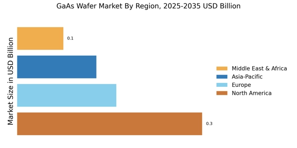
North America is the largest market for GaAs wafers, holding approximately 45% of the global share. The region benefits from strong demand in telecommunications, consumer electronics, and automotive sectors, driven by advancements in 5G technology and IoT applications. Regulatory support for semiconductor manufacturing and R&D initiatives further catalyze growth, making it a key player in the global landscape. The United States leads the market, with major companies like Broadcom, Qorvo, and Skyworks Solutions driving innovation and production. The competitive landscape is characterized by significant investments in technology and infrastructure, ensuring a robust supply chain. The presence of leading firms enhances the region's capability to meet rising demand, solidifying its position as a global leader in GaAs wafer production.

Europe : Emerging Technology Powerhouse

Europe is witnessing a significant rise in the GaAs wafer market, accounting for approximately 25% of the global share. The region's growth is fueled by increasing investments in renewable energy, telecommunications, and automotive sectors. Regulatory frameworks promoting sustainable technologies and innovation are pivotal in driving demand for GaAs wafers, particularly in high-frequency applications. Germany and the Netherlands are the leading countries in this market, with companies like Aixtron SE and NXP Semiconductors playing crucial roles. The competitive landscape is marked by collaborations between industry and academia, fostering innovation. The presence of key players and supportive government policies positions Europe as a vital contributor to The GaAs Wafer Market.

Asia-Pacific : Rapid Growth and Expansion

Asia-Pacific is the second-largest market for GaAs wafers, holding around 20% of the global share. The region's growth is driven by the booming electronics sector, particularly in countries like Japan and South Korea, where demand for high-performance devices is surging. Government initiatives to boost semiconductor manufacturing and technological advancements are key regulatory catalysts supporting this growth. Japan and South Korea are at the forefront, with companies like Sumitomo Electric Industries and Mitsubishi Chemical Corporation leading the charge. The competitive landscape is characterized by rapid technological advancements and a focus on R&D. The presence of major players and a growing consumer base position Asia-Pacific as a critical region in The GaAs Wafer Market.

Middle East and Africa : Emerging Market Potential

The Middle East and Africa region is gradually emerging in the GaAs wafer market, currently holding about 10% of the global share. The growth is primarily driven by increasing investments in telecommunications and electronics, alongside government initiatives aimed at diversifying economies. Regulatory support for technology adoption and infrastructure development is crucial for fostering market growth in this region. Countries like South Africa and the UAE are showing potential, with a focus on enhancing local manufacturing capabilities. The competitive landscape is still developing, with opportunities for both local and international players to establish a foothold. As the region continues to invest in technology, it is poised for significant growth in the GaAs wafer market.

GaAs Wafer Market Regional Image

Key Players and Competitive Insights

Leading market players are investing heavily in research and development to expand their product lines, which will help the GaAs wafer market grow even more. Market participants are also undertaking various strategic activities to expand their footprint, with important market developments including new product launches, contractual agreements, mergers and acquisitions, higher investments, and collaboration with other organizations. To expand and survive in a more competitive and rising market climate, the GaAs wafer industry must offer cost-effective items.

Manufacturing locally to minimize operational costs is one of the key business tactics manufacturers use in the GaAs wafer industry to benefit clients and increase the market sector. Major players in the GaAs wafer market, including Semiconductor Wafer Inc (Taiwan), AXT, Inc. (U.S.), Freiberger Compound Materials GmbH (Germany), Xiamen Powerway Advanced Material Co., Ltd. (China), Sumitomo Electric Industries, Ltd. (Japan), and others, are attempting to increase market demand by investing in research and development operations.

AXT Inc (AXT) develops, manufactures, and supplies semiconductor substrates. The company's product portfolio includes indium phosphide (InP), germanium (Ge), GaAs wafer, boron trioxide (B2O3), and raw and purified gallium. It also offers products that include gallium-magnesium alloy and pyrolytic boron nitride (pBN) crucibles. AXT products find applications in areas such as light-emitting diodes (LEDs), fiber optic and wireless telecommunications, lasers, and solar cells for space and terrestrial photovoltaic applications. In April 2021, AXT, Inc. Supplied the First 8-Inch GaAs wafer to major customer.

The 8-inch GaAs wafer substrates, which are silicon-doped, n-type substrates, demonstrate low etch pit densities (EPD) and low levels of slip lines.

Okmetic Inc. manufactures silicon wafers. The Company produces silicon on GaAs wafer, epitaxial wafers, double-side polish wafers, semiconductor wafers, and other related wafers for the sensor and semiconductor industries. Okmetic offers its products throughout the world. In June 2022, Okmetic participated in the EU-wide Position II project that comprised 43 partners and 12 countries. By using available technology platforms for miniaturization, wireless connectivity, MEMS transducer technology, in-tip AD conversion, and encapsulation, the project aimed to create the next generation of smart catheters and implants. These platforms are available to a huge range of consumers and applications.

Key Companies in the GaAs Wafer Market market include

Industry Developments

May 2022: The MOSIS Service of Information Sciences Institute, University of Southern California, declared an MoU with WIN Semiconductors Corp. to accelerate the expansion of GaAs wafer and GaN monolithic microwave integrated circuits (MMICs) with WIN Semiconductors' GaAs wafer and GaN process technologies. The partnership will help the dedicated, innovative, and adequate design and prototyping flow via the multi-project wafer (MPW) projects with the MOSIS Service and WIN Semiconductors.

February 2022: ProAsia Semiconductor Corporation., a subsidiary of Optotech Corporation, Taiwan, announced its plan to invest NT USD 3 billion (USD 107.63 million) to make chips using third-generation semiconductor materials. The program will support the demand for the fast-growing electric vehicle, 5G, and green energy markets.

April 2021: AXT, Inc., a leading manufacturer of compound semiconductor substrate wafers, has developed and shipped its first 8-inch diameter GaAs wafer substrates to a major customer. The 8-inch GaAs substrates, which are silicon-doped, n-type substrates, demonstrate low etch pit densities (EPD) and low levels of slip lines.

Future Outlook

GaAs Wafer Market Future Outlook

The GaAs Wafer Market is projected to grow at a 10.46% CAGR from 2024 to 2035, driven by advancements in telecommunications, consumer electronics, and renewable energy applications.

New opportunities lie in:

  • Expansion into emerging markets with tailored GaAs solutions.
  • Development of high-efficiency solar cells utilizing GaAs technology.
  • Strategic partnerships with semiconductor manufacturers for innovative product lines.

By 2035, the GaAs Wafer Market is expected to achieve robust growth and increased market share.

Market Segmentation

GaAs Wafer Market Applications Outlook

  • Mobile Devices
  • Photovoltaic Devices
  • Wireless Communication
  • Optoelectronic Device
  • Aerospace & Defense
  • Others

GaAs Wafer Market Production Method Outlook

  • Vertical Gradient Freeze (VGF)
  • Liquid Encapsulated Czochralski (LEC)
  • Molecular Beam Epitaxy (MBE)
  • Metal Organic Vapor Phase Epitaxy (MOVPE)

Report Scope

MARKET SIZE 20240.62(USD Billion)
MARKET SIZE 20250.6849(USD Billion)
MARKET SIZE 20351.852(USD Billion)
COMPOUND ANNUAL GROWTH RATE (CAGR)10.46% (2024 - 2035)
REPORT COVERAGERevenue Forecast, Competitive Landscape, Growth Factors, and Trends
BASE YEAR2024
Market Forecast Period2025 - 2035
Historical Data2019 - 2024
Market Forecast UnitsUSD Billion
Key Companies ProfiledMarket analysis in progress
Segments CoveredMarket segmentation analysis in progress
Key Market OpportunitiesGrowing demand for high-frequency applications drives innovation in the GaAs Wafer Market.
Key Market DynamicsTechnological advancements drive demand for GaAs wafers in telecommunications and consumer electronics sectors.
Countries CoveredNorth America, Europe, APAC, South America, MEA

Market Highlights

Author
Aarti Dhapte
Team Lead - Research

She holds an experience of about 6+ years in Market Research and Business Consulting, working under the spectrum of Information Communication Technology, Telecommunications and Semiconductor domains. Aarti conceptualizes and implements a scalable business strategy and provides strategic leadership to the clients. Her expertise lies in market estimation, competitive intelligence, pipeline analysis, customer assessment, etc.

Leave a Comment

FAQs

What is the projected market valuation of the GaAs Wafer Market by 2035?

The GaAs Wafer Market is projected to reach a valuation of 1.852 USD Billion by 2035.

What was the market valuation of the GaAs Wafer Market in 2024?

In 2024, the GaAs Wafer Market was valued at 0.62 USD Billion.

What is the expected CAGR for the GaAs Wafer Market during the forecast period 2025 - 2035?

The expected CAGR for the GaAs Wafer Market during the forecast period 2025 - 2035 is 10.46%.

Which production method segment is projected to have the highest valuation in the GaAs Wafer Market?

The Metal Organic Vapor Phase Epitaxy (MOVPE) segment is projected to have the highest valuation, ranging from 0.25 to 0.75 USD Billion.

What are the key applications driving the GaAs Wafer Market?

Key applications driving the GaAs Wafer Market include Mobile Devices, Photovoltaic Devices, and Wireless Communication.

Which company is a leading player in the GaAs Wafer Market?

Broadcom, based in the US, is recognized as a leading player in the GaAs Wafer Market.

Download Free Sample

Kindly complete the form below to receive a free sample of this Report

Compare Licence

×
Features License Type
Single User Multiuser License Enterprise User
Price $4,950 $5,950 $7,250
Maximum User Access Limit 1 User Upto 10 Users Unrestricted Access Throughout the Organization
Free Customization
Direct Access to Analyst
Deliverable Format
Platform Access
Discount on Next Purchase 10% 15% 15%
Printable Versions