High Bandwidth Memory Market (2025 - 2035)

High Bandwidth Memory Market Size, Share and Research Report By Application (Servers, Networking, Consumer Electronics, Automotive, and Other Applications), By Region (North America, Europe, Asia-Pacific, And Rest Of The World) –Industry Forecast Till 2035
ID: MRFR/SEM/19987-HCR
200 Pages
Ankit Gupta
Last Updated: July 22, 2026
High Bandwidth Memory Market
Market Size
Forecast Period2025-2035
CAGR (2025-2035)24.0%
2025 Market SizeUSD 3.40 Billion
2035 Market SizeUSD 29.70 Billion
Key Players
SK Hynix
Samsung Electronics
Micron Technology
NVIDIA
TSMC
AMD
Opportunities
  • HBM4 and Hybrid-Bonding Architectures
  • Edge-Inference Hardware for Industrial and Automotive Platforms
  • Sovereign AI Infrastructure Programs

High Bandwidth Memory Market Summary

The High Bandwidth Memory Market reached an estimated USD 3.40 billion in 2025 and is projected to grow from USD 4.28 billion in 2026 to USD 29.70 billion by 2035, registering a CAGR of 24.0% during 2026–2035. Two converging forces are accelerating this trajectory: generative-AI training clusters that demand bandwidth exceeding 2.5 terabytes per second per stack, and government subsidy programs — collectively surpassing USD 110 billion across Asia-Pacific and North America — that are underwriting aggressive fab expansions for advanced memory packaging [1][2].

A decisive technology shift is underway. Conventional GDDR and DDR architectures can no longer keep pace with the data-movement requirements of transformer-scale models, pushing hyperscalers and silicon designers toward vertically stacked DRAM architectures paired with 2.5-D interposer packaging. SK Hynix alone committed over USD 14.6 billion to new HBM production lines between 2023 and 2025, while Samsung and Micron collectively earmarked an additional USD 11 billion in capacity investments [3][4]. The High Bandwidth Memory Market is effectively transitioning from a specialty component niche into a foundational pillar of AI infrastructure.

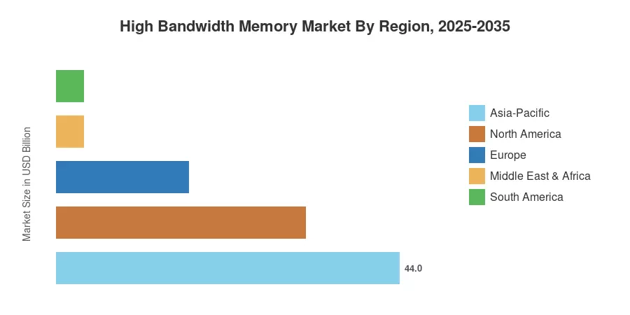
Asia-Pacific commands approximately 44.0% of the High Bandwidth Memory Market, driven by fabrication hubs in South Korea, Japan, and China. The region is also the fastest-growing, projected at a 24.8% CAGR through 2035. North America holds roughly a 32.0% share, anchored by hyperscaler procurement from major cloud providers. Europe accounts for about 17.0%, with automotive-grade deployments in Germany and France gaining momentum. As edge inference expands into vehicles and industrial gateways, the High Bandwidth Memory Market will continue broadening well beyond its data-center origins.

Key Report Takeaways

• By Technology

  • HBM3 captured roughly 49.0% of revenue in 2025, reflecting its dominant position across current-generation AI accelerators.
  • HBM3E is forecast to expand at a CAGR of 24.6% during 2026–2035 as next-generation GPU platforms transition to higher-bandwidth stacks.

• By Application

  • Servers accounted for approximately 63.0% of the High Bandwidth Memory Market in 2025, driven by cloud and hyperscale AI workloads.
  • Automotive and transportation applications are projected to grow at a 28.4% CAGR, fueled by autonomous-driving compute requirements.

• By Region

  • Asia-Pacific led the High Bandwidth Memory Market with a 44.0% share in 2025.
  • North America held a 32.0% share, supported by sustained hyperscaler capital expenditure cycles.
  • South America and the Middle East & Africa together represent emerging procurement frontiers for edge-inference hardware.


Market Size and Forecast (2021–2035)

Market Research Future employs a triangulated methodology combining bottom-up revenue analysis from semiconductor vendor financials, top-down demand modeling from AI-compute deployment forecasts, and primary interviews with procurement executives at cloud hyperscalers, OEMs, and foundry partners. All historical figures are reconciled against publicly reported shipment data and ASP trends.
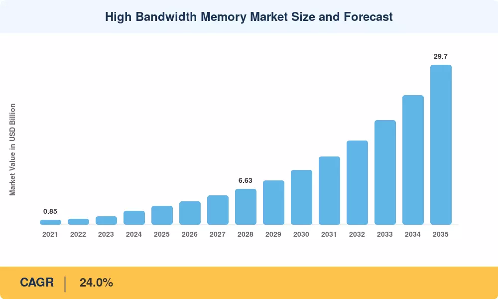
High Bandwidth Memory Market Size and Forecast
Our Impact
Enabled $4.3B Revenue Impact for Fortune 500 and Leading Multinationals
Partnering with 2000+ Global Organizations Each Year
30K+ Citations by Top-Tier Firms in the Industry

Driver Impact Analysis

Driver ~% Impact on CAGR Geographic Relevance Impact Timeline
Generative-AI training compute expansion 30–35% Global Short-term (≤2 yr)
Government semiconductor subsidies 15–20% Asia-Pacific, North America Medium-term (2–4 yr)
Autonomous-vehicle compute requirements 10–12% North America, Europe Long-term (≥4 yr)
Cloud-hyperscaler capital expenditure cycles 12–15% North America, Asia-Pacific Short-term (≤2 yr)
Advanced 2.5-D packaging capacity expansion 8–10% Asia-Pacific Medium-term (2–4 yr)
Edge-inference proliferation in IoT gateways 5–7% Europe, Asia-Pacific Long-term (≥4 yr)
Sovereign AI and supply-chain regionalization 5–8% Global Medium-term (2–4 yr)


Generative-AI Training Compute Expansion

Large-language-model training runs now routinely consume tens of thousands of GPUs for months at a time, and each accelerator card requires multiple HBM stacks. NVIDIA's H100 and B200 platforms each pair the GPU die with six to eight HBM3E stacks, meaning a single 10,000-GPU cluster can absorb over 60,000 individual memory stacks. Meta's 2024 infrastructure plan alone called for 350,000 H100-equivalent GPUs, translating into more than USD 2.1 billion in embedded HBM value [1][6]. This demand concentration gives memory suppliers pricing power rarely seen in the broader DRAM industry.

Government Semiconductor Subsidies

The U.S. CHIPS and Science Act allocated USD 52.7 billion for domestic semiconductor manufacturing and R&D, with specific provisions for advanced packaging facilities critical to HBM production. South Korea's K-Semiconductor Strategy committed approximately USD 450 billion in combined public-private investment through 2030, with SK Hynix and Samsung as primary beneficiaries [2][9]. These subsidies directly reduce the capital-expenditure burden on memory makers and accelerate time-to-volume production for next-generation stacks.

Cloud-Hyperscaler Capital Expenditure

Alphabet, Amazon, Microsoft, and Meta collectively spent over USD 160 billion on capital infrastructure in 2024, with AI-related hardware accounting for an increasing share. Each successive generation of custom AI silicon — from Google's TPU v5p to Amazon's Trainium2 — specifies higher-capacity HBM configurations [11][14]. The High Bandwidth Memory Market benefits directly from these procurement cycles because memory content per server rack increases with each refresh.

Autonomous-Vehicle Compute Requirements

Level-4 autonomous-driving platforms from Waymo, Cruise, and emerging Chinese AV players require onboard inference throughput approaching 2,000 TOPS. Meeting this target with acceptable power budgets pushes automotive chipmakers toward HBM integration rather than conventional LPDDR solutions. The automotive segment's 28.4% projected CAGR reflects the convergence of regulatory mandates for advanced driver-assistance and the rising sensor-data processing loads from lidar and camera fusion [10][15].


Restraints Impact Analysis

Restraint ~% Negative Impact on CAGR Geographic Relevance Impact Timeline
Advanced packaging capacity bottlenecks –8 to –10% Global Short-term (≤2 yr)
Export-control regimes bifurcating supply chains –5 to –7% Asia-Pacific, North America Medium-term (2–4 yr)
High ASPs limiting adoption in cost-sensitive segments –4 to –6% South America, MEA Long-term (≥4 yr)
Thermal management complexity in dense stacks –3 to –5% Global Medium-term (2–4 yr)
Concentrated supplier base creating single-point risks –3 to –4% Global Long-term (≥4 yr)


Advanced Packaging Capacity Bottlenecks

Producing HBM requires through-silicon-via (TSV) drilling, micro-bump bonding, and silicon-interposer fabrication — processes where global capacity remains structurally limited. TSMC's CoWoS advanced-packaging output was reportedly oversubscribed by 2–3× through 2025, forcing customers into allocation-based purchasing [3]. Until new packaging lines reach volume production in late 2027, supply constraints will continue capping shipment growth below theoretical demand levels for the High Bandwidth Memory Market.

Export-Control Regimes

U.S. Commerce Department restrictions on advanced semiconductor exports to China — updated in October 2023 and tightened further in 2024 — directly affect HBM shipments because stacks integrated into high-end AI accelerators fall within controlled performance thresholds [13]. These controls fragment global supply chains, force Chinese customers toward domestic alternatives of lower bandwidth, and introduce compliance costs that ripple through the High Bandwidth Memory Market's distribution channels.

High Average Selling Prices

HBM3E stacks command ASPs roughly 5–6× higher than equivalent-capacity DDR5 modules, making them economically viable primarily for data-center and high performance applications. Consumer-electronics and mid-tier networking segments remain priced out, limiting the addressable market's breadth and slowing volume-driven cost reductions that would otherwise accelerate broader adoption [16].


High Bandwidth Memory Market Opportunities

HBM4 and Hybrid-Bonding Architectures

The transition from thermocompression bonding to hybrid (copper-to-copper) bonding promises denser interconnects and lower per-bit costs. SK Hynix targets HBM4 volume production by 2026, with bandwidth exceeding 1.5 TB/s per stack, opening performance headroom that current HBM3E cannot deliver[3].

Edge-Inference Hardware for Industrial and Automotive Platforms

As autonomous vehicles and smart factory gateways demand real-time inference at the edge, compact HBM stacks with lower power envelopes present a significant growth vector. Automotive Tier-1 suppliers such as Bosch and Continental are qualifying HBM-equipped system-on-chips for production vehicles slated for 2028–2030 model years[10].

Sovereign AI Infrastructure Programs

Governments across the EU, India, Japan, and the Gulf states are funding national AI compute clusters, each requiring thousands of HBM-equipped accelerators. The EU AI Factories initiative, backed by EUR 1.5 billion, mandates procurement of European-assembled AI hardware, creating localized demand for the High Bandwidth Memory Market[13].

Memory-as-a-Service and Disaggregated Architectures

CXL (Compute Express Link) memory pooling enables operators to provision HBM capacity across multiple compute nodes dynamically. This architectural shift introduces subscription-based memory procurement models, potentially expanding the buyer base beyond hardware OEMs to include cloud operators billing memory by the hour[14].

Emerging-Market Data-Center Buildouts

Brazil, Saudi Arabia, and South Africa are investing in hyperscale data centers to support sovereign cloud mandates. Saudi Arabia's NEOM technology zone alone has earmarked USD 5 billion for AI-ready infrastructure, creating net-new demand for the High Bandwidth Memory Market in regions historically served by conventional DDR architectures[18].


High Bandwidth Memory Market Future Outlook

AI-Compute Scaling and Memory-Wall Economics

The "memory wall" — the growing gap between processor speed and memory bandwidth — will intensify through 2035 as AI models scale beyond ten trillion parameters. Each model-size doubling roughly doubles HBM demand per training cluster, creating a structural demand multiplier for the High Bandwidth Memory Market. IEA projections estimate global data-center electricity consumption could reach 1,000 TWh by 2030, with memory subsystems consuming an increasing share [1][21].

Platform Economics and Vertical Integration

GPU designers are moving toward tighter co-engineering with memory vendors — NVIDIA's joint development with SK Hynix on custom HBM3E configurations exemplifies this trend. By 2030, vertically integrated memory-compute platforms may emerge where the distinction between processor and memory blurs, reshaping the competitive dynamics of the High Bandwidth Memory Market [4][14].

Packaging Innovation Supercycle

Hybrid bonding, glass-core interposers, and chiplet-based architectures will redefine how HBM stacks are integrated. TSMC's roadmap through 2028 includes system-on-wafer approaches that can accommodate 12-high and 16-high DRAM stacks, potentially tripling per-package bandwidth. This packaging supercycle will be a decisive factor in whether the High Bandwidth Memory Market can sustain its growth trajectory into the 2030s [3][22].

Sustainability and Energy-Efficiency Imperatives

ESG reporting requirements and corporate carbon pledges are pushing operators to favor memory technologies that deliver more compute per watt. HBM's bandwidth-per-watt advantage over GDDR — roughly 3–4× at equivalent throughput — positions it favorably as regulators in the EU and California mandate energy-efficiency disclosures for data-center operators [21][23].


High Bandwidth Memory Market Segmentation

By Application

Segment Key Metric Primary Demand Driver
Servers 63.0% share (2025) AI training and inference workloads
Networking CAGR 22.5% (2026–2035) High-throughput switch and router ASICs
High-Performance Computing USD 0.38 Billion (2025) Scientific simulation and modeling
Consumer Electronics CAGR 19.8% (2026–2035) Premium gaming consoles and VR headsets
Automotive and Transportation CAGR 28.4% (2026–2035) Autonomous-driving compute platforms


The High Bandwidth Memory Market's server segment retains its leadership position because AI training clusters at hyperscale data centers represent the largest single pool of HBM procurement. Each next-generation accelerator increases the number of HBM stacks per board — from four on NVIDIA A100 to eight on B200 — compounding server-segment revenue with every product cycle. Automotive and transportation is the fastest-growing application as Level-3+ autonomy mandates increase onboard memory bandwidth requirements by an order of magnitude compared to ADAS-only vehicles [10][15].

By Technology

Segment Key Metric Primary Demand Driver
HBM2 USD 0.12 Billion (2025) Legacy HPC and networking equipment
HBM2E 14.0% share (2025) Mid-life AI accelerator platforms
HBM3 49.0% share (2025) Current-generation GPU deployments
HBM3E CAGR 24.6% (2026–2035) Next-gen data-center accelerators
HBM4 CAGR 35.0% (2026–2035) Future ultra-bandwidth AI platforms


HBM3 dominates the High Bandwidth Memory Market today because it is the production-qualified standard for current flagship accelerators. HBM3E — offering approximately 50% higher bandwidth per pin — is ramping into volume for platforms launching in 2026–2027, while HBM4's hybrid-bonding architecture positions it as the long-term growth engine once qualification completes around 2027–2028 [3][7].

By Memory Capacity Per Stack

Segment Key Metric Primary Demand Driver
4 GB CAGR 8.5% (2026–2035) Legacy design-ins winding down
8 GB USD 0.52 Billion (2025) Mid-range HPC and networking
16 GB 35.2% share (2025) Mainstream AI accelerator configurations
24 GB CAGR 26.0% (2026–2035) High-capacity training GPU stacks
32 GB and above CAGR 28.7% (2026–2035) Next-gen ultra-high-capacity platforms


The 16 GB tier holds the largest share in the High Bandwidth Memory Market because it aligns with the standard stack configuration across current AI accelerator families. Rapid migration toward 24 GB and 32 GB+ stacks is underway as model sizes expand and inference workloads demand larger working-memory footprints per device [7][8].

By Processor Interface

Segment Key Metric Primary Demand Driver
GPU 59.2% share (2025) AI training and graphics workloads
CPU CAGR 20.5% (2026–2035) Memory-bandwidth-sensitive server CPUs
AI Accelerator/ASIC CAGR 27.4% (2026–2035) Custom silicon for inference at scale
FPGA USD 0.08 Billion (2025) Prototyping and low-latency applications
Other Interfaces CAGR 18.0% (2026–2035) Emerging neuromorphic and analog compute


GPUs command the largest share of the High Bandwidth Memory Market's processor-interface segmentation because NVIDIA, AMD, and Intel GPU platforms collectively account for the majority of AI-compute shipments. Custom AI accelerators and ASICs — including Google TPUs, Amazon Trainium, and a growing roster of startup chips — represent the fastest growth vector as cloud operators diversify away from GPU-only architectures [11][14].


Regional Market Share Analysis

Region Key Metric Primary Investment Themes
Asia-Pacific 44.0% share (2025) Fab expansion, packaging innovation, government subsidies
North America 32.0% share (2025) Hyperscaler procurement, CHIPS Act funding
Europe 17.0% share (2025) Automotive-grade HBM, EU AI Factories
South America 3.5% share (2025) Sovereign cloud buildouts
Middle East & Africa 3.5% share (2025) AI-ready data centers, Vision 2030 programs
Total 100%

The High Bandwidth Memory Market's regional hierarchy reflects the global concentration of semiconductor fabrication, hyperscale data-center fleets, and government subsidy programs.


North America

Country Key Metric Key Driver
US 27.5% of global market Hyperscaler CapEx and CHIPS Act incentives
Canada CAGR 22.8% (2026–2035) AI research hubs in Toronto and Montreal
Mexico USD 0.06 Billion (2025) Nearshoring of semiconductor assembly operations


The United States dominates North American demand because the headquarters and primary data-center fleets of Alphabet, Amazon, Microsoft, and Meta are concentrated domestically. CHIPS Act disbursements exceeding USD 30 billion in committed awards by mid-2025 are catalyzing advanced packaging facilities in Arizona and Texas, strengthening the domestic supply chain for the High Bandwidth Memory Market [2][11].

Europe

Country Key Metric Key Driver
Germany 6.2% of global market Automotive OEM compute upgrades
UK CAGR 23.5% (2026–2035) AI safety research cluster investments
France USD 0.14 Billion (2025) National AI strategy procurement
Italy CAGR 21.8% (2026–2035) Industrial automation platforms
Spain USD 0.05 Billion (2025) Cloud landing-zone expansions
Nordic Countries CAGR 22.4% (2026–2035) Green data-center deployments
Russia USD 0.03 Billion (2025) Domestic chip import-substitution efforts
Rest of Europe CAGR 21.0% (2026–2035) Distributed AI inference nodes


Europe's High Bandwidth Memory Market growth is anchored by automotive compute upgrades in Germany, where BMW, Mercedes-Benz, and Volkswagen are specifying HBM-equipped SoCs for Level-3 and Level-4 autonomous platforms. The EU Chips Act, with EUR 43 billion in public-private funding, further supports advanced packaging R&D across the continent [15][19].

Asia-Pacific

Country Key Metric Key Driver
South Korea 18.5% of global market SK Hynix and Samsung production hubs
China CAGR 23.2% (2026–2035) Domestic AI accelerator development
Japan USD 0.32 Billion (2025) Rapidus fab and packaging partnerships
India CAGR 26.5% (2026–2035) National semiconductor mission
ASEAN USD 0.08 Billion (2025) Assembly and test facility expansion
Rest of Asia-Pacific CAGR 22.0% (2026–2035) Emerging cloud infrastructure


Asia-Pacific's dominance in the High Bandwidth Memory Market stems from the region housing all three major HBM manufacturers' primary fabrication sites. South Korea's K-Semiconductor Strategy and Japan's USD 25 billion semiconductor investment package are expanding interposer and TSV capacity, while India's USD 10 billion semiconductor mission is attracting back-end packaging operations [2][9][20].

South America

Country Key Metric Key Driver
Brazil 2.2% of global market Hyperscale data-center construction
Argentina CAGR 20.5% (2026–2035) University AI research clusters
Rest of South America USD 0.02 Billion (2025) Early-stage cloud adoption


Brazil's High Bandwidth Memory Market growth is tied to cloud-region openings by AWS and Oracle in São Paulo and Campinas. Government-backed AI strategies are still nascent, but private-sector procurement is creating a beachhead for HBM-equipped inference servers [18].

Middle East & Africa

Country Key Metric Key Driver
Saudi Arabia CAGR 25.0% (2026–2035) NEOM AI infrastructure investments
UAE 1.2% of global market Abu Dhabi sovereign AI programs
South Africa USD 0.01 Billion (2025) Academic and government HPC clusters
Egypt CAGR 19.5% (2026–2035) Smart-city digital infrastructure
Rest of MEA USD 0.01 Billion (2025) Nascent data-center development


Saudi Arabia and the UAE are the primary demand centers in this region, with sovereign wealth funds channeling billions into AI compute infrastructure. The High Bandwidth Memory Market benefits as these nations procure cutting-edge GPU clusters for national AI models and smart-city platforms [18].


High Bandwidth Memory Market By Region, 2025-2035

Competitive Benchmarking

The High Bandwidth Memory Market is highly concentrated, with an estimated top-three share exceeding 90% and a Herfindahl-Hirschman Index (HHI) well above 2,500. SK Hynix, Samsung Electronics, and Micron Technology are the only companies currently mass-producing HBM stacks, giving the market an oligopolistic structure. Beyond these three, the competitive landscape includes key integration partners, packaging houses, and IP licensors whose technologies enable HBM deployment.

Company Est. Revenue Share Range Key Offerings for High Bandwidth Memory Market Strategic Positioning
SK Hynix ~35–42% HBM3, HBM3E, HBM4 development Market leader; primary NVIDIA supplier
Samsung Electronics ~28–35% HBM3E 12-high stacks, custom bandwidth configs Vertically integrated with foundry and packaging
Micron Technology ~12–18% HBM3E 8-high and 12-high stacks Third entrant scaling aggressively
NVIDIA ~2–4% (IP/co-dev) Co-designed HBM specifications for GPU platforms Demand architect; defines stack requirements
TSMC ~1–3% (packaging) CoWoS interposer and advanced packaging services Sole-source for leading-edge 2.5-D integration
AMD ~1–2% (specification) MI300X and MI400 HBM integration Growing AI accelerator market share
Intel ~1–2% (specification) Gaudi3 and Falcon Shores HBM integration Re-entering AI accelerator competition
ASE Technology ~1–2% (packaging) Advanced fan-out and 2.5-D packaging Key OSAT for HBM module assembly
Rambus <1% (IP licensing) HBM PHY and memory interface IP Licensing model spans multiple manufacturers
Broadcom <1% (ASIC design) Custom AI ASICs with HBM interfaces Designs HBM-equipped chips for hyperscalers

Recent News & Developments

  • SK Hynix (March 2025): Began mass production of 12-high HBM3E stacks delivering 1.18 TB/s bandwidth, securing allocation commitments from NVIDIA for next-generation Blackwell Ultra platforms [7].
  • TSMC (August 2024): Expanded CoWoS advanced packaging capacity by building a new facility in Chiayi, Taiwan, aimed at relieving the interposer bottleneck constraining the High Bandwidth Memory Market [3].
  • NVIDIA (March 2024): Unveiled the B200 GPU platform specifying eight HBM3E stacks per accelerator, doubling per-chip memory bandwidth versus the H100 generation [6].
  • SK Hynix (June 2023): Announced successful development of HBM4 prototype using hybrid-bonding technology, targeting volume production in 2026 [3].
  • European Commission (April 2023): Approved the EU Chips Act with EUR 43 billion in public-private investment, including dedicated funding for advanced memory packaging R&D [19].


High Bandwidth Memory Market Report Scope

Parameter Detail
Market Scope Global High Bandwidth Memory Market — by Application, Technology, Memory Capacity Per Stack, Processor Interface, and Geography
Study Period 2021–2035
CAGR (2026–2035) 24.0%
Base Year Market Size USD 3.40 Billion (2025)
Forecast Endpoint USD 29.70 Billion (2035)
Fastest Growing Segments Automotive & Transportation (application); HBM4 (technology); 32 GB+ (capacity); AI Accelerator/ASIC (processor interface); Asia-Pacific (region)
Companies Profiled SK Hynix, Samsung Electronics, Micron Technology, NVIDIA, TSMC, AMD, Intel, ASE Technology, Rambus, Broadcom
Valuation Currency USD Billion


FAQs

How do HBM procurement lead times affect AI infrastructure deployment timelines?
Lead times for HBM3E currently stretch 40–50 weeks because advanced packaging capacity remains constrained. AI infrastructure operators must secure allocations 12–18 months ahead of deployment [3].
What role does CXL play in extending HBM utilization across disaggregated compute architectures?
CXL 3.0 enables memory pooling across multiple hosts, allowing shared HBM resources to serve workloads dynamically. This reduces per-node memory overprovisioning by an estimated 25–30% [14].
How do export controls on advanced chips create secondary effects on HBM demand patterns?
U.S. export restrictions redirect Chinese demand toward domestically produced lower-bandwidth alternatives, fragmenting global HBM supply chains. This bifurcation elevates ASPs in unrestricted markets [13].
What quality and reliability standards apply to automotive-grade HBM stacks?
Automotive HBM must meet AEC-Q100 Grade 2 qualification covering –40°C to 105°C operating ranges. Qualification cycles typically add 12–18 months versus commercial-grade timelines [10].
How does hybrid bonding in HBM4 differ technically from thermocompression bonding in HBM3E?
Hybrid bonding uses direct copper-to-copper interconnects at sub-1-micron pitch, eliminating solder bumps entirely. This enables 2× higher interconnect density and lower parasitic resistance [22].
What is the total cost of ownership difference between HBM-equipped and GDDR-equipped inference servers?
HBM servers cost 2–3× more upfront but deliver 4× bandwidth per watt, reducing total inference cost per query by approximately 35–45% at scale [16].
Are there viable alternatives to silicon interposers for HBM integration?
Glass-core interposers and embedded bridge technologies are emerging alternatives that offer lower warpage and larger panel sizes. Volume production is expected by 2028–2029 [22].    
Author
Author
Author Profile
Ankit Gupta LinkedIn
Team Lead - Research
Ankit Gupta is a seasoned market intelligence and strategic research professional with over six plus years of experience in the ICT and Semiconductor industries. With academic roots in Telecom, Marketing, and Electronics, he blends technical insight with business strategy. Ankit has led 200+ projects, including work for Fortune 500 clients like Microsoft and Rio Tinto, covering market sizing, tech forecasting, and go-to-market strategies. Known for bridging engineering and enterprise decision-making, his insights support growth, innovation, and investment planning across diverse technology markets.

Research Approach


Secondary Research

The secondary research process involved comprehensive analysis of semiconductor industry databases, technical standards publications, peer-reviewed engineering journals, and authoritative technology organizations. Key sources included the Institute of Electrical and Electronics Engineers (IEEE), International Electron Devices Meeting (IEDM), Semiconductor Industry Association (SIA), Electronic Industries Alliance (EIA), Joint Electron Device Engineering Council (JEDEC), European Semiconductor Industry Association (ESIA), Korea Semiconductor Industry Association (KSIA), Taiwan Semiconductor Industry Association (TSIA), US Department of Commerce Bureau of Industry and Security, International Trade Administration (ITA), Organization for Economic Cooperation and Development (OECD) ICT Statistics, World Semiconductor Trade Statistics (WSTS), IC Insights, Gartner Semiconductor Research, SEMI (Semiconductor Equipment and Materials International), and national technology ministry reports from South Korea (Ministry of Trade, Industry and Energy), Japan (Ministry of Economy, Trade and Industry), and Taiwan (Industrial Development Bureau).

Wafer production statistics, memory technology roadmaps, fabrication capacity data, JEDEC HBM standards documentation (JESD235 series), AI/ML infrastructure deployment metrics, and competitive landscape analysis for HBM2, HBM2E, HBM3, and HBM3E memory technologies were all gathered from these sources.


Primary Research

In order to gather both qualitative and quantitative insights, supply-side and demand-side stakeholders were interviewed during the primary research process. CEOs, VPs of Memory Product Development, heads of Advanced Packaging Engineering, and commercial directors from memory semiconductor producers, OSATs (Outsourced Semiconductor Assembly and Test), and suppliers of advanced packaging technology were examples of supply-side sources. Chief Technology Officers, VPs of Infrastructure Engineering, procurement leads from hyperscale cloud providers (AWS, Google Cloud, Microsoft Azure), AI/ML platform businesses, data center operators, networking equipment OEMs, and automotive electronics manufacturers were among the demand-side sources. In addition to gathering information on high-volume manufacturing yields, price dynamics, and supply chain allocation strategies between AI accelerator and traditional server markets, primary research verified HBM stack height and bandwidth evolution roadmaps and validated technology migration timescales.

Primary Respondent Breakdown:

By Designation: C-level Primaries (40%), Director Level (25%), Others (35%)

By Region: North America (38%), Europe (22%), Asia-Pacific (32%), Rest of World (8%)


Market Size Estimation

Revenue mapping and bit-shipment volume analysis across HBM generations were used to determine the global market valuation. The methodology comprised:

Finding more than 25 important producers and technology licensors in Taiwan, Asia-Pacific, Europe, and North America

Product mapping for next-generation HBM4, HBM2, HBM2E, HBM3, and HBM3E technologies

Analysis of quarterly sales for HBM product portfolios, both reported and modeled

Coverage of producers accounting for 85–90% of the world market in 2024

Extrapolation of segment-specific valuations by application (servers, networking, consumer electronics, automotive) using top-down (memory manufacturer revenue validation, OSAT packaging revenue correlation) and bottom-up (AI accelerator and server GPU unit shipments × HBM content per device × blended ASP by HBM generation) approaches

Download Free Sample

Kindly complete the form below to receive a free sample of this Report

Download PDF ×

We do not share your information with anyone. However, we may send you emails based on your report interest from time to time. You may contact us at any time to opt-out.